MEMS device and manufacturing method thereof

A manufacturing method and device technology, applied in the direction of electric solid-state devices, semiconductor devices, semiconductor/solid-state device components, etc., can solve the problems of large packaging volume and low integration of MEMS devices, achieve fast signal transmission speed, and improve device performance , to achieve the effect of miniaturization

Pending Publication Date: 2022-07-01
NINGBO SEMICON INT CORP
View PDF0 Cites 0 Cited by
  • Summary
  • Abstract
  • Description
  • Claims
  • Application Information

AI Technical Summary

Problems solved by technology

[0005] The purpose of the present invention is to provide a kind of MEMS device and its manufacturing method, at least solve the technical problems such as large packaging volume and low integration degree of the manufactured MEMS device

Method used


Image

  • MEMS device and manufacturing method thereof
  • MEMS device and manufacturing method thereof
  • MEMS device and manufacturing method thereof

Examples


Embodiment 1

[0037] Embodiment 1 of the present invention provides a method for fabricating a MEMS device, comprising the following steps:

[0038]S01: Provide a logic chip, the logic chip includes a substrate and a CMOS circuit on the substrate, a first structural layer is formed on the logic chip, and a first isolation trench is formed on the first structural layer;

[0039] S02: Provide a bulk acoustic wave filter, the bulk acoustic wave filter includes: a carrier substrate, a support layer formed on the surface of the carrier substrate, and a piezoelectric material that surrounds a second cavity with the carrier substrate and the support layer A laminated structure, the piezoelectric laminated structure includes a second electrode, a piezoelectric layer, and a first electrode stacked in sequence;

[0040] S03: The BAW filter is bonded on the first structural layer on the logic chip, so that the first isolation groove is sandwiched between the logic chip and the BAW filter to form a fir...

Embodiment 2

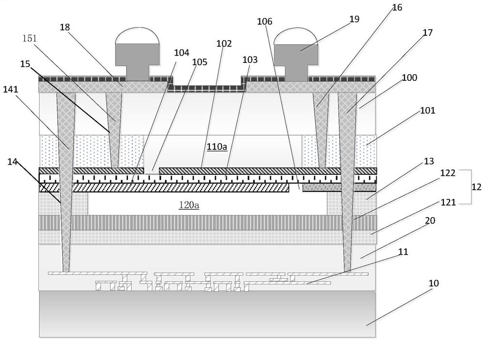
[0094] This embodiment 2 provides a MEMS device, figure 1 A schematic structural diagram of a MEMS device of the second embodiment is shown, please refer to figure 1 , the MEMS device includes:

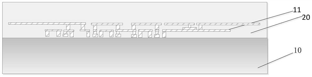
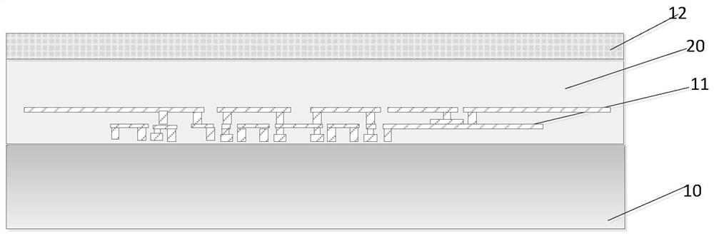
[0095] a logic chip, the logic chip includes a CMOS circuit 11;

[0096] a first structural layer 13, the first structural layer 13 is located above the logic chip;

[0097] A bulk acoustic wave filter, the bulk acoustic wave filter is located above the first structural layer, and there is a bonding interface between the bulk acoustic wave filter and the first structural layer; the bulk acoustic wave filter includes a bearing lining the bottom 100, the acoustic reflection structure on the surface of the carrier substrate 100, and the piezoelectric laminated structure on the acoustic reflection structure;

[0098] The first structure layer 13 has a first cavity 120a, and the effective resonance region of the piezoelectric laminated structure is located in the first cavity 120a.

[...


PUM

PropertyMeasurementUnit
Thicknessaaaaaaaaaa

Abstract

The invention relates to an MEMS device and a manufacturing method thereof, and the method comprises the steps: providing a logic chip which comprises a substrate and a CMOS circuit located on the substrate, and forming a first structure layer with a first isolation groove on the logic chip; providing a bulk acoustic wave filter, wherein the bulk acoustic wave filter comprises a bearing substrate, a supporting layer formed on the surface of the bearing substrate, and a piezoelectric laminated structure which forms a second cavity with the bearing substrate and the supporting layer; the bulk acoustic wave filter is bonded on the first structure layer, so that the first isolation groove is clamped between the logic chip and the bulk acoustic wave filter to form a first cavity; an effective resonance region of the piezoelectric laminated structure is located in the first cavity. The first structure layer with the first isolation groove is formed on the logic chip, the bulk acoustic wave filter is bonded to the first structure layer through the bonding technology, the first cavity is formed by the bulk acoustic wave filter and the first structure layer, vertical integration of the bulk acoustic wave filter and the logic chip is achieved in the device manufacturing stage, the manufacturing technology is simplified, and the manufacturing cost is reduced. The packaging volume of the whole system is reduced, and the integration level is greatly improved.

Description

technical field [0001] The invention relates to the field of MEMS device manufacturing, in particular to a MEMS device and a manufacturing method thereof. Background technique [0002] Micro-Electro-Mechanical System (MEMS) and integrated circuit (IC) are currently the two most important development areas in the semiconductor industry. Driven by the rapid development of global technology, the integration of MEMS and IC has become a It is an inevitable trend, and there are three integration methods: monolithic integration, semi-hybrid (bonding) integration and hybrid integration; monolithic integration refers to the fabrication of MEMS structure and CMOS on one chip; hybrid integration refers to the fabrication of MEMS and IC in different On the die, and then packaged in a package, the MEMS bare chip with bumps is connected to the IC chip in the form of flip-chip bonding or wire bonding to form SIP; semi-hybrid is to use three-dimensional integration technology to realize MEM...

Claims


Application Information

Patent Timeline
IPC IPC(8): B81C1/00B81B7/00B81B7/02H03H3/02H03H9/02
CPCB81C1/00238B81C1/00301B81B7/007B81B7/0006B81B7/02H03H3/02H03H9/02B81C1/00B81B7/00H03H9/0547H03H9/564H03H2003/021H03H2003/027
Inventor 李伟黄河罗海龙
Owner NINGBO SEMICON INT CORP
Why Eureka
Try Eureka