Image sensor and fabricating method thereof

An image sensor and pattern technology, which can be used in semiconductor/solid-state device manufacturing, image communication, electrical solid-state devices, etc., and can solve problems such as reducing the resolution of the fill factor area.

Inactive Publication Date: 2010-05-26
DONGBU HITEK CO LTD
View PDF1 Cites 0 Cited by
  • Summary
  • Abstract
  • Description
  • Claims
  • Application Information

AI Technical Summary

Problems solved by technology

[0006] Therefore, horizontal CMOS image sensors require additional area for photodiode formation, which reduces fill factor area and limits resolution

Method used


Image

  • Image sensor and fabricating method thereof
  • Image sensor and fabricating method thereof
  • Image sensor and fabricating method thereof

Examples


Embodiment Construction

[0018] Hereinafter, a manufacturing method thereof according to a preferred embodiment of the present invention will be described in detail with reference to the accompanying drawings.

[0019] In describing embodiments of the present invention, it should be understood that when a layer is referred to as being "on / over" another layer, it can be directly on another layer or indirectly through an intervening layer present between the layers. on another floor.

[0020] In the drawings, the thickness and size of layers are exaggerated, omitted or simplified for better understanding and clarity of the present invention. In addition, the size of an element does not necessarily mean its actual size.

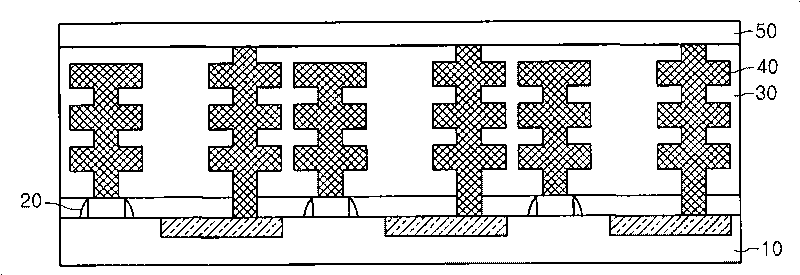
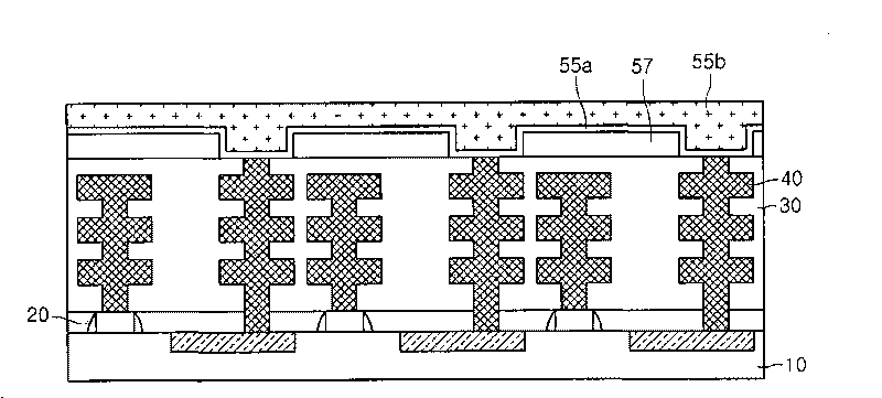
[0021] Figure 1 to Figure 9 is a cross-sectional view illustrating a method for manufacturing an image sensor according to an embodiment of the present invention.

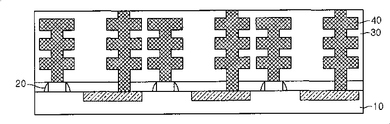
[0022] Such as figure 1 As shown, an interlayer dielectric film 30 including a metal line 40 is formed on a semicondu...


PUM


Abstract

An image sensor and a method of fabricating an image sensor. An image sensor may include a readout circuitry arranged over a semiconductor substrate, an interlayer dielectric film provided with metal lines arranged over a semiconductor substrate, and/or a lower electrode arranged over a interlayer dielectric film such that a lower electrode may be connected to metal lines. An image sensor may include a first-type conductive layer pattern arranged over a lower electrode, an intrinsic layer arranged over a surface of a semiconductor substrate such that an intrinsic layer may substantially cover a first-type conductive layer pattern. An image sensor may include a second-type conductive layer arranged over an intrinsic layer. A method of fabricating an image sensor may include a patterned n-type amorphous silicon layer which may be treated with N2O plasma. A method of fabricating an image sensor may include H2 annealing.

Description

[0001] This application claims priority from Korean Patent Application No. 10-2008-0096404 filed on Oct. 1, 2008, the entire contents of which are hereby incorporated by reference. technical field [0002] The invention relates to an image sensor and a manufacturing method thereof. Background technique [0003] A general image sensor is a semiconductor device that converts an optical image into an electrical signal. Such image sensors mainly include charge coupled device (charge coupled device, CCD) image sensors and complementary metal oxide semiconductor (complementary metal oxide silicon, CMOS) image sensors. [0004] The CMOS image sensor includes photodiodes and MOS transistors in unit pixels to detect electrical signals in each unit pixel in a switching mode, thereby realizing an image. [0005] Such a CMOS image sensor has a structure in which a photodiode portion that converts an optical signal into an electrical signal and a transistor portion that processes the el...

Claims


Application Information

Patent Timeline
Patent Type & Authority Applications(China)
IPC IPC(8): H04N5/335H04N3/15H01L27/146H01L21/82
CPCH01L27/14665H01L27/14634H01L27/146
Inventor 李汉春郑伍珍
Owner DONGBU HITEK CO LTD
Why Eureka
Try Eureka