System and method for manufacturing micro light emitting diode display

A technology for light emitting diodes and display panels, which is applied to the equipment for forming miniature light emitting diode panels, and the field of forming miniature light emitting diode display panels, can solve the problems of time-consuming, industrial infeasibility and the like

Pending Publication Date: 2022-04-15
吳伯仁 +1
View PDF2 Cites 0 Cited by
  • Summary
  • Abstract
  • Description
  • Claims
  • Application Information

AI Technical Summary

Problems solved by technology

The mass transfer problem still exists as millions of tiny LEDs must be individually picked from the bonding substrate to the receiving

Method used


Image

  • System and method for manufacturing micro light emitting diode display
  • System and method for manufacturing micro light emitting diode display
  • System and method for manufacturing micro light emitting diode display

Examples


Embodiment Construction

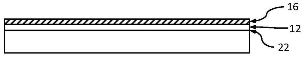
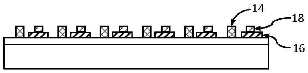
[0057] As used herein, the term "substrate" generally refers to a plate formed of semiconductor or non-semiconductor material. Examples of such semiconducting or non-semiconducting materials include, but are not limited to, monocrystalline silicon, silicon carbide, gallium arsenide, indium phosphide, sapphire, ceramics, glass, and printed circuit boards. Such substrates may typically be found and / or handled in semiconductor fabrication facilities. The epitaxial substrate refers to a substrate provided for epitaxial growth in semiconductor manufacturing equipment. A bonded substrate refers to a substrate having circuitry and bonding pads thereon to receive electronic components.

[0058] As for the substrate, a one-layer or multi-layer structure may be formed on the substrate. Many different types of layers are known in the art, and the term "substrate" as used herein is intended to encompass a chip on which all types of layers may be formed. One or more layers formed on a s...


PUM


Abstract

The invention discloses a structure and a manufacturing method of a display panel, and micro light emitting diodes can be manufactured very accurately and efficiently by using a chip-by-chip mode, mainly a separation technology. Firstly, after an epitaxial process, a light-emitting diode epitaxial wafer is manufactured into a miniature light-emitting diode chip; then, a bonding substrate with a driving circuit is provided for the light emitting diode epitaxial wafer. Each of the light emitting diode chips may then be simultaneously or sequentially fixed to the substrate chip by chip, and each of the light emitting diode chips may be simultaneously or sequentially transferred using a separation technique. The light emitting diode epitaxial wafer itself may also be provided as a light emitting diode display substrate.

Description

technical field [0001] The present invention relates to a technology of a micro light emitting diode (Micro LED) display panel and a method for forming a micro light emitting diode display panel; in particular, it relates to a technology of an apparatus for forming a micro light emitting diode panel. Background technique [0002] Micro-LEDs are considered to be the next high-tech displays after traditional thin-film-transistor liquid-crystal displays (TFT LCD) and organic light-emitting diode (OLED) displays. The advantages of miniature LEDs inherited from conventional LEDs include low power consumption, high brightness, short response time, and long lifetime. Sony (SONY) announced and manufactured a 55-inch Crystal LED TV (Crystal LED TV) assembled from miniature light-emitting diodes in 2012, of which more than 6 million miniature light-emitting diodes are used as a high-resolution display with a million-level contrast ratio. High-rate pixels, more than 140% color TV broa...

Claims


Application Information

Patent Timeline
IPC IPC(8): H01L25/16H01L27/15H01L33/50H01L33/32G09F9/33
Inventor 吴伯仁曾家彬
Owner 吳伯仁
Why Eureka
Try Eureka