PCB and pressing method thereof
A substrate and prepreg technology, applied in multilayer circuit manufacturing, printed circuit components, etc., can solve problems such as low production efficiency, production pollution, and large interlayer deviation, so as to improve production efficiency, avoid processes, and reduce lamination layers. biased effect
- Summary
- Abstract
- Description
- Claims
- Application Information
AI Technical Summary
Problems solved by technology
Method used
Image

Examples
no. 1 example
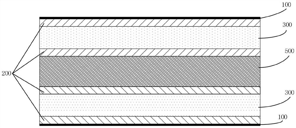
[0047] Please refer to attached figure 2 , attached image 3 And attached Image 6 , the present invention provides a PCB and its pressing method, comprising the following steps:
[0048] S01: Cut the two substrates 300 into a predetermined size, and perform inner layer patterning on the substrates 300 .
[0049] S02: Use an automatic optical inspection machine to detect and repair the open circuit, short circuit, gap and residual copper of the substrate 300 .
[0050] Specifically, S02 includes the following steps:
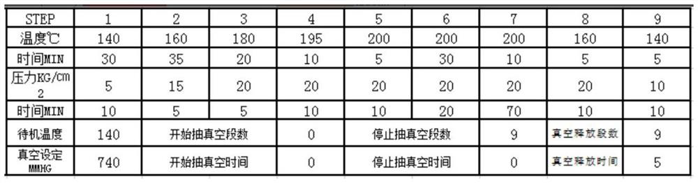
[0051]S21: Use the LDI exposure machine to transfer and fabricate the inner layer pattern, and control the layer deviation of the inner layer within 20 microns. Wherein, pattern transfer refers to the pattern transfer of the photographic master plate to the copper-clad foil substrate. In addition, the layer deviation control of the inner layer can be realized by setting the layer deviation accuracy of the LDI exposure machine, and other processes of the inn...
no. 2 example
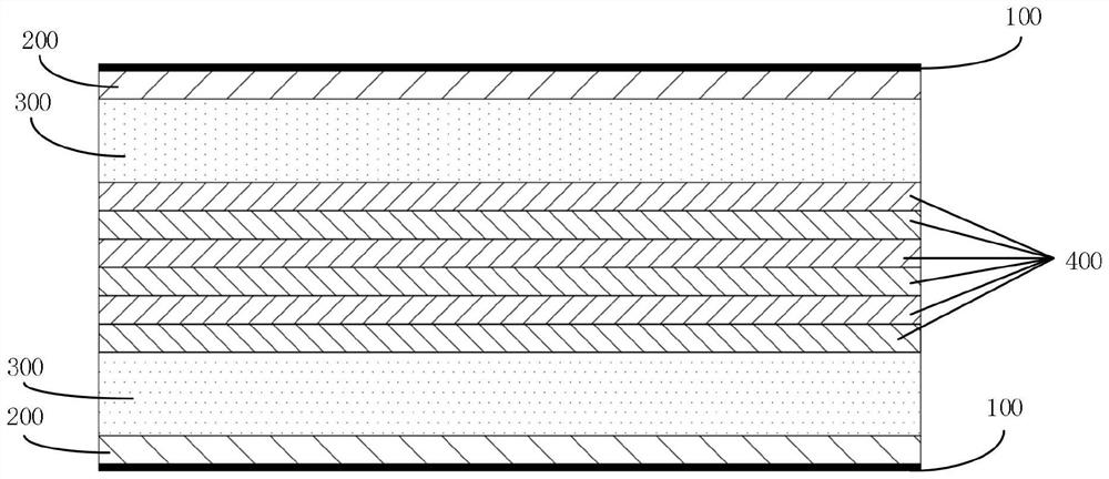
[0067] Please refer to the attached Figure 4 , attached Figure 5 And attached Image 6 , the present invention provides a PCB and its pressing method, comprising the following steps:
[0068] S01: Cut the two substrates 300 into a predetermined size, and perform inner layer patterning on the substrates 300 .
[0069] S02: Use an automatic optical inspection machine to detect and repair the open circuit, short circuit, gap and residual copper of the substrate 300 .
[0070] Specifically, S02 includes the following steps:
[0071] S21: Use the LDI exposure machine to transfer and fabricate the inner layer pattern, and control the layer deviation of the inner layer within 20 microns. In addition, the layer deviation control of the inner layer can be realized by setting the layer deviation accuracy of the LDI exposure machine, and other processes of the inner layer are processed according to the control method of the multilayer board.
[0072] S03 : Punching the substrate 3...
PUM
| Property | Measurement | Unit |
|---|---|---|
| thickness | aaaaa | aaaaa |
Abstract
Description
Claims
Application Information
 - R&D
- Intellectual Property
- Life Sciences
- Materials
- Tech Scout
- Unparalleled Data Quality
- Higher Quality Content
- 60% Fewer Hallucinations
Browse by: Latest US Patents, China's latest patents, Technical Efficacy Thesaurus, Application Domain, Technology Topic, Popular Technical Reports.
© 2025 PatSnap. All rights reserved.Legal|Privacy policy|Modern Slavery Act Transparency Statement|Sitemap|About US| Contact US: help@patsnap.com