Semiconductor structure and forming method thereof

A semiconductor and gate structure technology, applied in the field of semiconductor structure and its formation, can solve problems such as poor device performance, achieve the effects of ensuring dimensional stability, simplifying the process, and improving electrical performance

Pending Publication Date: 2022-03-04
SEMICON MFG INT (SHANGHAI) CORP +1
View PDF0 Cites 0 Cited by
  • Summary
  • Abstract
  • Description
  • Claims
  • Application Information

AI Technical Summary

Problems solved by technology

When the existing lithography technology cannot meet the corresponding process requirements, a series of problems are likely to occur, resulting in poor performance of the devices formed by the existing semiconductor process

Method used


Image

  • Semiconductor structure and forming method thereof
  • Semiconductor structure and forming method thereof
  • Semiconductor structure and forming method thereof

Examples


Embodiment Construction

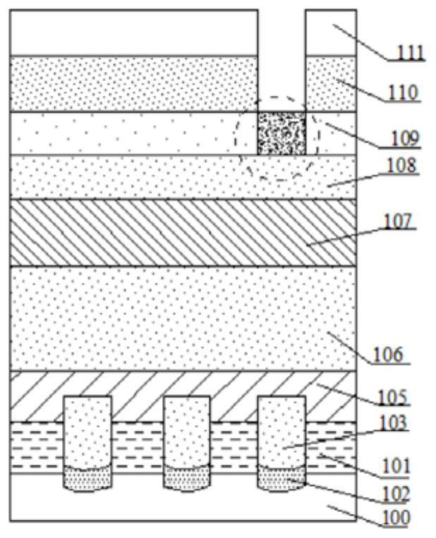
[0019] Currently formed devices still suffer from poor performance. The reasons for the poor performance of the device are analyzed in conjunction with a method of forming a semiconductor structure.

[0020] Figure 1 to Figure 9 , is a structural schematic diagram corresponding to each step in a method for forming a semiconductor structure.

[0021] like figure 1 As shown, a substrate is provided, and the substrate includes a substrate 100, a gate structure 101 on the substrate 100, a source-drain doped layer 102 on both sides of the gate structure 101, and a 101 on both sides and covering the interlayer dielectric layer 103 of the source-drain doped layer 102; on the gate structure 101 and the interlayer dielectric layer 103, a dielectric layer 106, a mask layer 107, a dielectric layer 108, and Graphic definition layer 109 . Form a first anti-reflection material layer (not shown) on the pattern definition layer 109; form a first photoresist layer 111 on the first anti-re...


PUM


Abstract

The invention discloses a semiconductor structure and a forming method thereof, and the method comprises the steps: providing a substrate which comprises a substrate, a gate structure located on the substrate, source and drain doping layers located at the two sides of the gate structure, and interlayer dielectric layers which are located at the two sides of the gate structure and cover the source and drain doping layers; a mask layer is formed on the gate structure and the interlayer dielectric layer, a first opening is formed in the mask layer, and the first opening corresponds to the source-drain doping layer, extends in the extending direction of the gate structure and is continuous; forming a sacrificial layer, wherein the sacrificial layer fills a part of the first opening; and etching the interlayer dielectric layer corresponding to the first opening which is not filled by the sacrificial layer to form a first groove exposing the source-drain doping layer. According to the method, the electrical performance of the device is improved, the process is simplified, and the cost is reduced.

Description

technical field [0001] Embodiments of the present invention relate to the field of semiconductor manufacturing, and in particular, to a semiconductor structure and a method for forming the same. Background technique [0002] In semiconductor manufacturing, with the development trend of VLSI, the feature size of integrated circuits continues to decrease. In particular, the feature size is rapidly developing in the direction of micron and nanometer, and the line width of the pattern will become thinner and thinner, which puts forward higher requirements for semiconductor technology. [0003] In the subsequent process of the integrated circuit, the transfer of the integrated circuit pattern is usually realized by photolithography technology (Lithograph). However, the thinner the line width of the pattern of the integrated circuit, the higher the process requirements for the photolithography technology. When the existing photolithography technology cannot meet the correspondin...

Claims


Application Information

Patent Timeline
Patent Type & Authority Applications(China)
IPC IPC(8): H01L21/336H01L21/027H01L21/033H01L29/78G03F1/80
CPCH01L29/66636H01L29/66795H01L29/785H01L29/7838H01L21/0276H01L21/0332G03F1/80
Inventor 赵炳贵
Owner SEMICON MFG INT (SHANGHAI) CORP
Why Eureka
Try Eureka