TOPCon battery phosphorus diffusion process
A phosphorus diffusion and process technology, applied in the direction of circuits, photovoltaic power generation, electrical components, etc., can solve the problems of difficult to form N/N+ structure field passivation, restrict the conversion efficiency of TOPCon technology, and destroy the integrity of the tunneling oxide layer. Achieve the effects of fewer grain boundaries, improved efficiency, and improved carrier selection
- Summary
- Abstract
- Description
- Claims
- Application Information
AI Technical Summary
Problems solved by technology
Method used
Image

Examples
Embodiment 1
[0027] A TOPCon battery phosphorus diffusion process, comprising the following steps:
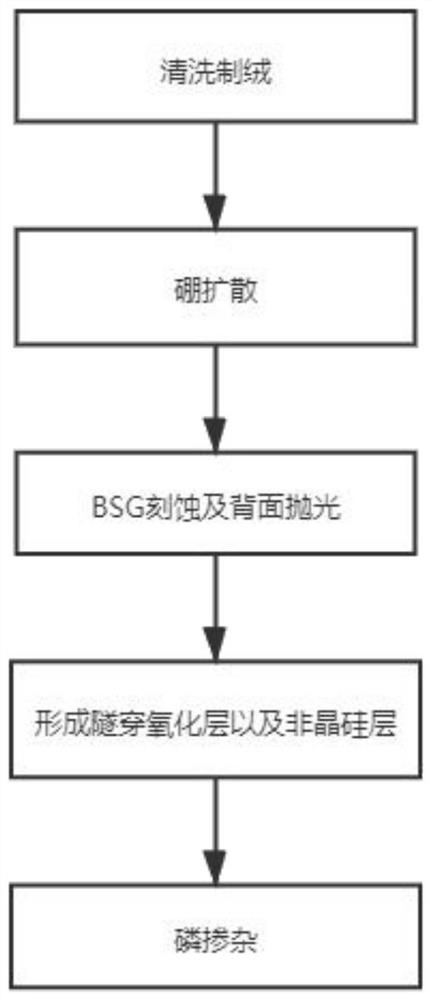
[0028] Step 1: Select N-type silicon wafer as the substrate material, and produce a pyramid-like surface structure on the surface of the silicon wafer by cleaning and texturing;
[0029] Step 2: performing boron diffusion on the front surface of the silicon wafer;
[0030] Step 3: Perform BSG etching and back polishing on the silicon wafer;
[0031] Step 4: Form a tunneling oxide layer on the back of the silicon wafer by nitric acid oxidation, thermal oxidation or LPCVD preparation method, the thickness of the tunneling oxide layer is 1-2nm; and form an amorphous silicon layer on the tunneling oxide layer, the The thickness of the amorphous silicon layer is 100-140nm.
[0032] Step 5: Phosphorus doping is carried out on the amorphous silicon layer on the back side by means of extended temperature rise-constant temperature advancement-cooling advancement, so that the doped amorphous silico...
Embodiment 2
[0041] A TOPCon battery phosphorus diffusion process, comprising the following steps:
[0042] Step 1: Select N-type silicon wafer as the substrate material, and produce a pyramid-like surface structure on the surface of the silicon wafer by cleaning and texturing;
[0043] Step 2: performing boron diffusion on the front surface of the silicon wafer;
[0044] Step 3: Perform BSG etching and back polishing on the silicon wafer;
[0045] Step 4: Form a tunneling oxide layer on the back of the silicon wafer by nitric acid oxidation, thermal oxidation or LPCVD preparation method, the thickness of the tunneling oxide layer is 1-2nm; and form an amorphous silicon layer on the tunneling oxide layer, the The thickness of the amorphous silicon layer is 100-140nm.
[0046] Step 5: Phosphorus doping is carried out on the amorphous silicon layer on the back side by means of extended temperature rise-constant temperature advancement-cooling advancement, so that the doped amorphous silico...
Embodiment 3
[0055] A TOPCon battery phosphorus diffusion process, comprising the following steps:
[0056] Step 1: Select N-type silicon wafer as the substrate material, and produce a pyramid-like surface structure on the surface of the silicon wafer by cleaning and texturing;
[0057] Step 2: performing boron diffusion on the front surface of the silicon wafer;
[0058] Step 3: Perform BSG etching and back polishing on the silicon wafer;
[0059] Step 4: Form a tunneling oxide layer on the back of the silicon wafer by nitric acid oxidation, thermal oxidation or LPCVD preparation method, the thickness of the tunneling oxide layer is 1-2nm; and form an amorphous silicon layer on the tunneling oxide layer, the The thickness of the amorphous silicon layer is 100-140nm.
[0060] Step 5: Phosphorus doping is carried out on the amorphous silicon layer on the back side by means of extended temperature rise-constant temperature advancement-cooling advancement, so that the doped amorphous silico...
PUM
| Property | Measurement | Unit |
|---|---|---|
| thickness | aaaaa | aaaaa |
| thickness | aaaaa | aaaaa |
Abstract
Description
Claims
Application Information
 - R&D
- Intellectual Property
- Life Sciences
- Materials
- Tech Scout
- Unparalleled Data Quality
- Higher Quality Content
- 60% Fewer Hallucinations
Browse by: Latest US Patents, China's latest patents, Technical Efficacy Thesaurus, Application Domain, Technology Topic, Popular Technical Reports.
© 2025 PatSnap. All rights reserved.Legal|Privacy policy|Modern Slavery Act Transparency Statement|Sitemap|About US| Contact US: help@patsnap.com