Method for forming LaNiO3 thin film and method for manufacturing device
A thin film and device technology, applied in the field of LaNiO3 thin film, can solve the problems of increased film resistivity, etc., and achieve the effect of improved wettability and excellent film coating
- Summary
- Abstract
- Description
- Claims
- Application Information
AI Technical Summary
Problems solved by technology
Method used
Image
Examples
Embodiment 1
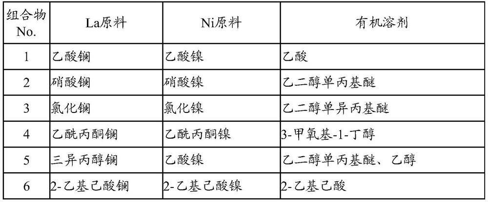
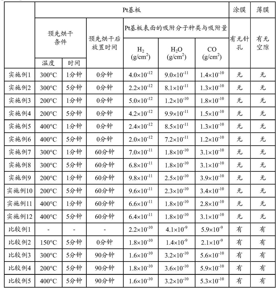
[0054] On a (100) plane-oriented Si substrate with a size of 17mm×17mm, SiO is sequentially stacked 2 layer, TiO 2 layer and Pt layer (top layer). The Pt layer was sputtered with a Pt source at room temperature under an argon atmosphere, and after film formation, no heat treatment was performed in an argon atmosphere. This substrate (hereinafter, referred to as a Pt plate.) was placed on a hot plate heated at 300° C. for 1 minute, and prebaked in the air. After the preliminary drying, the Pt substrate was cooled, and immediately the molecular species adsorbed on the surface of the Pt substrate was measured by thermal desorption gas analysis (Thermal Desorption Spectroscopy, hereinafter referred to as TDS method). On the other hand, the above-mentioned Pt substrate was pre-baked under the same conditions as above, and the Pt substrate was immediately moved to a spin coater without being placed in the atmosphere, and the composition No. shown in Table 1 was spin-coated on the ...
Embodiment 2
[0056] After pre-baking the same Pt substrate as in Example 1 at 300° C. for 5 minutes using the same heating plate as in Example 1, the Pt substrate was cooled, and the molecular species adsorbed on the surface of the Pt substrate was immediately measured by the TDS method. On the other hand, the above-mentioned Pt substrate was pre-baked under the same conditions as above, and the Pt substrate was immediately moved to a spin coater without being placed in the atmosphere, and the composition No. shown in Table 1 was spin-coated on the Pt substrate. .2. Next, in the same manner as in Example 1, drying, temporary sintering, and firing are performed to form LaNiO 3 film.
Embodiment 3
[0058] After pre-baking the same Pt substrate as in Example 1 at 200° C. for 1 minute using the same heating plate as in Example 1, the Pt substrate was cooled, and the molecular species adsorbed on the surface of the Pt substrate was immediately measured by the TDS method. On the other hand, the above-mentioned Pt substrate was pre-baked under the same conditions as above, and the Pt substrate was immediately moved to a spin coater without being placed in the atmosphere, and the composition No. shown in Table 1 was spin-coated on the Pt substrate. .3. Next, in the same manner as in Example 1, drying, temporary sintering, and firing are performed to form LaNiO 3 film.
PUM
| Property | Measurement | Unit |
|---|---|---|
| particle diameter | aaaaa | aaaaa |
| electrical resistivity | aaaaa | aaaaa |
| pore size | aaaaa | aaaaa |
Abstract
Description
Claims
Application Information
 - Generate Ideas
- Intellectual Property
- Life Sciences
- Materials
- Tech Scout
- Unparalleled Data Quality
- Higher Quality Content
- 60% Fewer Hallucinations
Browse by: Latest US Patents, China's latest patents, Technical Efficacy Thesaurus, Application Domain, Technology Topic, Popular Technical Reports.
© 2025 PatSnap. All rights reserved.Legal|Privacy policy|Modern Slavery Act Transparency Statement|Sitemap|About US| Contact US: help@patsnap.com


