Structure of deep ultraviolet light emitting diode and preparation method thereof
A light-emitting diode, deep ultraviolet light technology, applied in semiconductor devices, electrical components, circuits, etc., can solve the problems of insufficient luminous purity, low mobility, poor crystal quality, etc., to expand the scope of application, improve luminous efficiency, The effect of improving luminous efficiency
- Summary
- Abstract
- Description
- Claims
- Application Information
AI Technical Summary
Problems solved by technology
Method used
Image

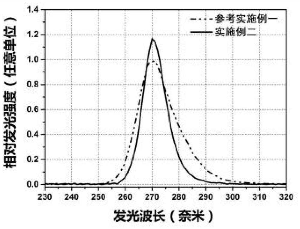
Examples
Embodiment 2
[0061] This specific embodiment is to prepare UVC light-emitting diodes, and the specific steps are:
[0062] (1) Use an MOCVD machine, heat up to 800°C, and feed TMAl and NH at 50Torr 3 and H 2 , forming 25nm low-temperature AlN on a sapphire substrate;
[0063] (2) Raise the temperature to 1270°C and feed TMAl and NH at 50Torr 3 and H 2 , forming 3μm high temperature AlN;
[0064] (3) Cool down to 1070°C and feed TMAl, TMGa, SiH at 50Torr 4 , NH 3 and H 2 , forming 2 μm N-type Al 0.6 Ga 0.4 N ohmic contact layer, where SiH 4 It is an N-type dopant, and the Si doping concentration is 4E+19cm -3 ;
[0065] (4) Lower the temperature to 1030°C and lower the pressure to 30Torr to feed TMAl, TMGa, SiH 4 , NH 3 and H 2 , forming Si-doped Al b Ga 1-b N / AlN / Al c Ga 1-c N interface planarized multilayer structure, in which, controlling the Al b Ga 1-b The thickness of N is 1-5nm, the thickness of AlN layer is 1-2nm, Al c Ga 1-c The thickness of the N layer is 1-5...
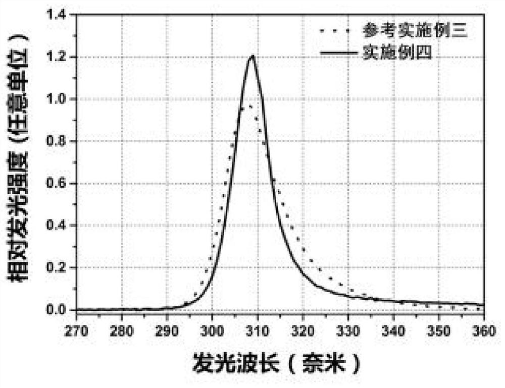
Embodiment 4
[0084] This specific embodiment is to prepare UVB light-emitting diode, and concrete steps are:
[0085] (1) Use an MOCVD machine, heat up to 800°C, and feed TMAl and NH at 50Torr 3 and H 2 , forming 25nm low-temperature AlN on a sapphire substrate;
[0086] (2) Raise the temperature to 1270°C and feed TMAl and NH at 50Torr 3 and H 2 , forming 3μm high temperature AlN;
[0087] (3) Cool down to 1070°C and feed TMAl, TMGa, SiH at 50Torr 4 , NH 3 and H 2 , forming 2 μm N-type Al 0.5 Ga 0.5 N ohmic contact layer, where SiH 4 It is an N-type dopant, and the Si doping concentration is 4E+19cm -3 ;
[0088] (4) Lower the temperature to 1030°C and lower the pressure to 30Torr to feed TMAl, TMGa, SiH 4 , NH 3 and H 2 , forming Si-doped Al b Ga 1-b N / AlN / Al c Ga 1-c N interface planarized multilayer structure, in which, controlling the Al b Ga 1-b The thickness of N is 1-5nm, the thickness of AlN layer is 1-2nm, Al c Ga 1-c The thickness of the N layer is 1-5nm; and...
PUM
| Property | Measurement | Unit |
|---|---|---|
| Thickness | aaaaa | aaaaa |
| Thickness | aaaaa | aaaaa |
| Thickness | aaaaa | aaaaa |
Abstract
Description
Claims
Application Information
 - R&D
- Intellectual Property
- Life Sciences
- Materials
- Tech Scout
- Unparalleled Data Quality
- Higher Quality Content
- 60% Fewer Hallucinations
Browse by: Latest US Patents, China's latest patents, Technical Efficacy Thesaurus, Application Domain, Technology Topic, Popular Technical Reports.
© 2025 PatSnap. All rights reserved.Legal|Privacy policy|Modern Slavery Act Transparency Statement|Sitemap|About US| Contact US: help@patsnap.com