
Laminated photovoltaic device and production method thereof

A photovoltaic device and stacking technology, applied in photovoltaic power generation, semiconductor devices, electrical components, etc., can solve the problems of high series resistance of devices and low tunnel junction tunneling efficiency, etc., to reduce series resistance, improve tunneling efficiency, reduce The effect of the overall series resistance of the device

Pending Publication Date: 2021-09-28
LONGI GREEN ENERGY TECH CO LTD
View PDF4 Cites 1 Cited by
  • Summary
  • Abstract
  • Description
  • Claims
  • Application Information

AI Technical Summary

Problems solved by technology

[0005] The invention provides a laminated photovoltaic device and a production method, aiming to solve the problems of low tunnel junction tunneling efficiency and high overall series resistance of the laminated photovoltaic device in which the lower battery unit is a crystalline silicon cell

Method used


Image

  • Laminated photovoltaic device and production method thereof
  • Laminated photovoltaic device and production method thereof
  • Laminated photovoltaic device and production method thereof

Examples


Embodiment Construction

[0043] The technical solutions in the embodiments of the present invention will be clearly and completely described below in conjunction with the accompanying drawings in the embodiments of the present invention. Obviously, the described embodiments are part of the embodiments of the present invention, but not all of them. Based on the implementation manners in the present invention, all other implementation manners obtained by persons of ordinary skill in the art without creative efforts fall within the protection scope of the present invention.

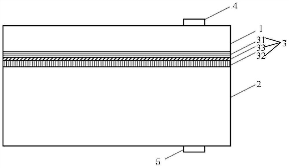
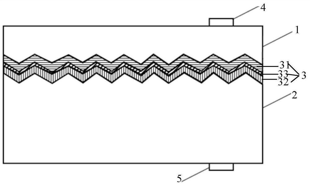
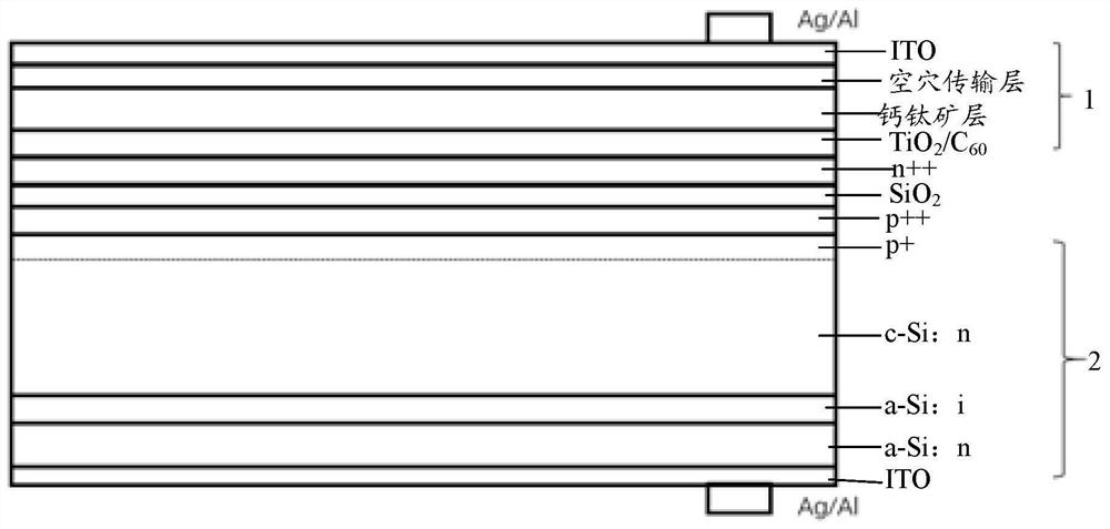
[0044] The inventor found in the research that: in the prior art, the main reason for the low efficiency of tunnel junction tunneling and high overall series resistance in stacked photovoltaic devices in which the lower cell is a crystalline silicon cell is that the slowly changing diffusion interface reduces the tunneling efficiency. The effective doping concentration on both sides of the junction interface and widen the tunneling d...


PUM

PropertyMeasurementUnit
dielectric strengthaaaaaaaaaa
thicknessaaaaaaaaaa
thicknessaaaaaaaaaa

Abstract

The invention provides a laminated photovoltaic device and a production method thereof, and relates to the technical field of photovoltaics. The laminated photovoltaic device comprises an upper-layer battery unit, a lower-layer battery unit, and a tunnel junction located between the upper-layer battery unit and the lower-layer battery unit; the lower-layer battery unit is a crystalline silicon battery; the tunnel junction comprises an upper crystalline silicon layer, a lower crystalline silicon layer, and an intermediate layer located between the upper crystalline silicon layer and the lower crystalline silicon layer; the upper crystalline silicon layer, the lower crystalline silicon layer and the intermediate layer are in direct contact, and the doping types of the upper crystalline silicon layer and the lower crystalline silicon layer are opposite; the doping concentration of the upper crystalline silicon layer at the interface with the intermediate layer and the doping concentration of the lower crystalline silicon layer at the interface with the intermediate layer are both greater than or equal to 10<18> cm<-3>; the intermediate layer comprises at least one dielectric layer; and the band gap width of the dielectric layer is greater than or equal to 3 eV. According to the invention, the efficiency of the laminated photovoltaic device is improved, the series resistance is reduced, and the peak tunnel current is improved.

Description

technical field [0001] The invention relates to the field of photovoltaic technology, in particular to a laminated photovoltaic device and a production method. Background technique [0002] Stacked photovoltaic devices can divide sunlight into multiple bands. From the front to the back, solar cells with gradually decreasing band gaps are used to absorb sunlight of different energies in order to broaden the spectral response band to sunlight and reduce energy loss. Therefore, stacked photovoltaic devices have broad application prospects. Stacked photovoltaic devices with crystalline silicon cells as the underlying cell unit have a large space for mass production. [0003] Tunnel junctions have strong transmission and recombination capabilities, and the thickness required to achieve high recombination rates is relatively thin. Therefore, tunnel junctions are usually used to connect battery cells in series in stacked photovoltaic devices. [0004] However, in the prior art, t...

Claims


Application Information

Patent Timeline
Patent Type & Authority Applications(China)
IPC IPC(8): H01L31/0687H01L31/0725H01L31/18H01L31/0236
CPCH01L31/0725H01L31/0687H01L31/18H01L31/0236Y02P70/50Y02E10/544H01L31/078H01L31/043H10K30/40H10K30/57H01L31/02363H01L31/1804
Inventor 吴兆徐琛李子峰
Owner LONGI GREEN ENERGY TECH CO LTD
Learn More