Underfill glue for electronic packaging device, preparation method and electronic packaging device

An underfill, electronic packaging technology, used in semiconductor/solid-state device parts, electrical solid devices, electrical components, etc., can solve the problems of increased system viscosity, reduced impact resistance of underfills, uneven dispersion, etc. Thermal expansion coefficient, low thermal expansion coefficient, easy dispersion effect

Active Publication Date: 2022-06-21
WUHAN CHOICE TECH CO LTD
View PDF6 Cites 0 Cited by
  • Summary
  • Abstract
  • Description
  • Claims
  • Application Information

AI Technical Summary

Problems solved by technology

However, blindly increasing the amount of toughening agent and silica filling in the underfill will increase the viscosity of the system, and the problem of uneven dispersion will occur if the silica content is too high, which will damage the fluidity of the underfill and cannot meet the requirements. Low viscosity and high fluidity requirements for sealing materials required for electronic packaging device installation
In addition, increasing the filling amount of the toughening agent will reduce the impact resistance of the underfill, making it difficult to maintain the adhesion of the underfill and electronic packaging devices to the substrate during transportation

Method used


Image

  • Underfill glue for electronic packaging device, preparation method and electronic packaging device
  • Underfill glue for electronic packaging device, preparation method and electronic packaging device
  • Underfill glue for electronic packaging device, preparation method and electronic packaging device

Examples


preparation example Construction

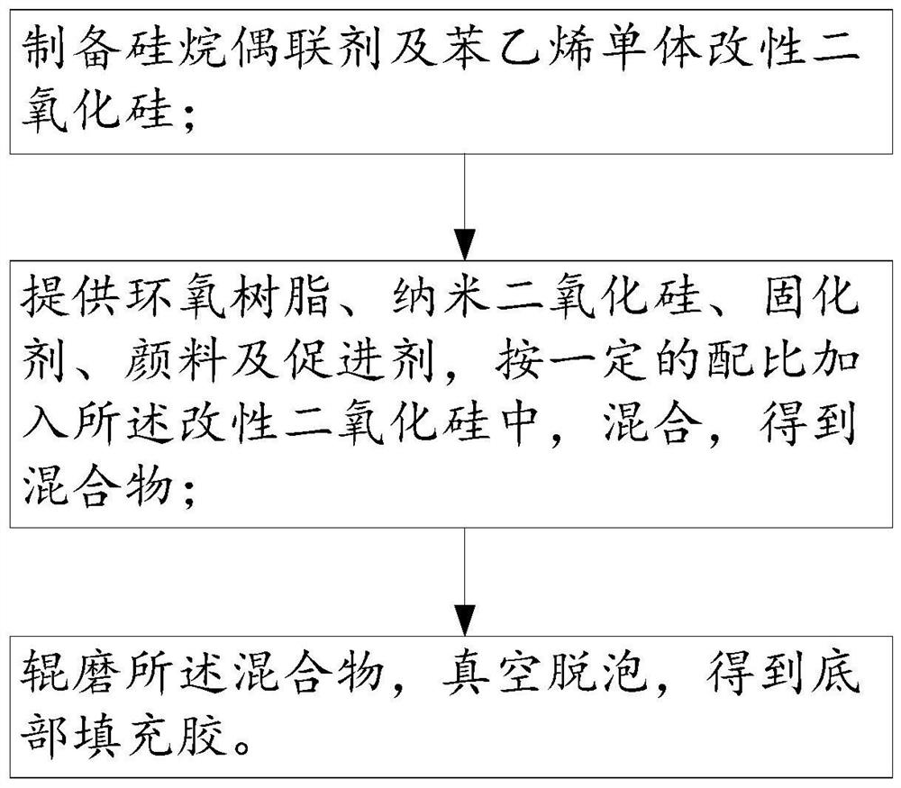
[0049] see figure 1 , the embodiment of the present application also provides a preparation method of an underfill for electronic packaging devices, comprising the following steps:

[0050] Step S1: preparing silane coupling agent and styrene monomer modified silica;

[0051] Step S2: providing epoxy resin, nano-silica, curing agent, pigment and accelerator, adding the silane coupling agent and styrene monomer modified silica in a certain proportion, and mixing to obtain a mixture; as well as

[0052] Step S3: Roll-milling the mixture and vacuum defoaming to obtain a low-expansion-coefficient underfill for electronic packaging devices.

[0053] In at least one embodiment, the step S1 is specifically:

[0054] Step S11: providing silica and adding it to the container;

[0055] Step S12: adding deionized water to the container, stirring and heating up to 70-90°C;

[0056] Step S13: add a silane coupling agent to the container, keep the temperature for a period of time T 1 ...

Embodiment 1

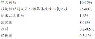
[0074] The underfill for electronic packaging devices in this embodiment is composed of the following raw materials by mass percentage:

[0075]

[0076] Wherein, the modified silica is obtained by the following method:

[0077] Weigh a certain weight of silica and add it to a four-necked flask, then add deionized water, stir and heat up to 80°C, then add γ-methacryloyloxypropyltrimethoxysilane, and keep the reaction for 12h to obtain modification Silica, wherein the mol ratio of silica to γ-methacryloyloxypropyltrimethoxysilane is 5:1;

[0078] A certain amount of styrene was slowly added dropwise at a rate of 2 drops per second. After the addition, the initiator ammonium persulfate was added dropwise, and the reaction was continued for 6 hours. The suspension was filtered and dried at a low temperature of 50 °C to obtain silane coupling agent and benzene. Ethylene monomer modified silica, wherein the molar ratio of modified silica, styrene and ammonium persulfate is 5:1:...

Embodiment 2

[0080] The underfill for electronic packaging devices in this embodiment is composed of the following raw materials by mass percentage:

[0081]

[0082] Wherein, the preparation method of the modified silica is the same as that in Example 1.


PUM

PropertyMeasurementUnit
particle diameteraaaaaaaaaa

Abstract

This application discloses an underfill for electronic packaging devices, which is mainly composed of the following raw materials in mass percentage: the underfill contains modified silicon dioxide, and the surface of the modified silicon dioxide is a polystyrene layer , can eliminate the hydrogen bond on the surface of the silica, so that there is no hydrogen bond on the surface of the modified silica, so that the force between the modified silica is small, has strong dispersibility, and is easy to disperse in the colloid. The filling amount of the modified silica in the low expansion coefficient underfill can be between 75-80% by mass, and there is no phenomenon of uneven dispersion, which can effectively reduce the thermal expansion coefficient of the underfill. In addition, the present application also discloses a method for preparing an underfill glue and an electronic packaging device.

Description

technical field [0001] The present application relates to the technical field of electronic packaging, and in particular, to an underfill for electronic packaging devices, a method for preparing the underfill for electronic packaging devices, and an electronic packaging device. Background technique [0002] Underfill is widely used in the circuit board packaging of portable electronic products such as MP3, USB, mobile phones, and Bluetooth. It is a key material in electronic device packaging technology. It is used to fill between the chip and the substrate to disperse the stress on the surface of the chip. It relieves the internal stress caused by the mismatch of thermal expansion coefficients of the chip, solder and substrate, reduces the stress impact caused by the difference in thermal expansion coefficient between the chip and the substrate, and improves the structural strength and reliability of electronic devices. [0003] With the continuous development of the electro...

Claims


Application Information

Patent Timeline
Patent Type & Authority Patents(China)
IPC IPC(8): C09J163/00C09J11/04H01L23/29
CPCC09J163/00C09J11/04H01L23/295C08K2201/011C08K3/36C08K9/06C08K9/04
Inventor 伍得王圣权王义廖述杭苏峻兴
Owner WUHAN CHOICE TECH CO LTD
Why Eureka
Try Eureka