
Multi-time overlay method

A simultaneous engraving and electronic technology, applied in the direction of microlithography exposure equipment, pattern surface photoplate making process, instruments, etc. Engraving accuracy and other issues

Inactive Publication Date: 2021-09-14
天津华慧芯科技集团有限公司
View PDF4 Cites 0 Cited by
  • Summary
  • Abstract
  • Description
  • Claims
  • Application Information

AI Technical Summary

Problems solved by technology

[0004] Multiple overlays require multiple exposure, etching, peeling, baking and other processes on the prepared Ti+Au mark, which will inevitably damage the shape of the mark to varying degrees and affect the mark detection signal At the same time, the traditional overlay still has the accumulation of deviations between two adjacent overlays, and the field splicing causes the relative position deviation of the mark and the graphic, thus affecting the overlay accuracy.

Method used


Image

  • Multi-time overlay method
  • Multi-time overlay method

Examples


Embodiment Construction

[0025] In order to enable those skilled in the art to better understand the solution of the present application, the technical solution in the embodiment of the application will be clearly and completely described below in conjunction with the accompanying drawings in the embodiment of the application. Obviously, the described embodiment is only It is an embodiment of a part of the application, but not all of the embodiments. Based on the embodiments in this application, all other embodiments obtained by persons of ordinary skill in the art without creative efforts shall fall within the scope of protection of this application.

[0026] It should be noted that the terms "comprising" and "having" and any variations thereof are intended to cover a non-exclusive inclusion, for example, a process, method, system, product or device comprising a series of steps or units is not necessarily limited to expressly instead of those steps or elements listed, may include other steps or eleme...


PUM


Abstract

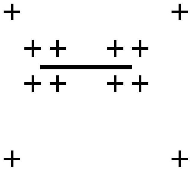
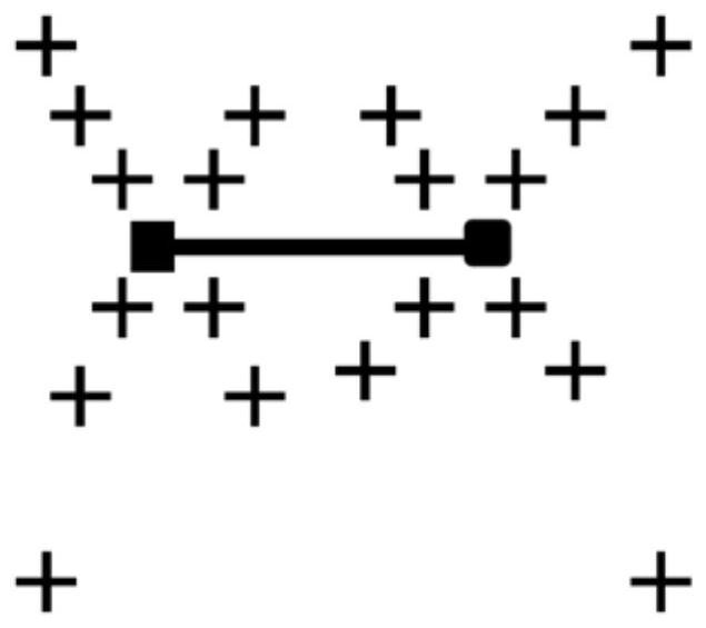
The invention discloses a multi-time overlay method, which belongs to the technical field of semiconductor micro-nano manufacturing, and comprises the following steps: cleaning a substrate; spin-coating an electronic resist on the substrate; performing electron beam exposure on the pattern, and meanwhile exposing the mark array near the pattern needing to be overlaid; developing the spin-coating electronic resist; etching the pattern and the mark which are overlayed for the first time at the same time; removing the electronic resist; spin-coating an electronic resist on the substrate; using the etching mark near the position needing to be overlayed in the last processing as an overlay mark, performing electron beam overlay on the pattern, and exposing the mark array at the same time; developing the spin-coating electronic resist; etching the pattern and the mark which are subjected to the last overlay at the same time; removing the electronic resist; and finishing the last time of overlay and etching. According to the method, the accumulation of two adjacent overlay deviations and the influence of the relative position deviation of the mark and the graph caused by field splicing are solved, the overlay precision is improved, and the problem that the overlay precision is influenced by the pollution of the mark can also be solved.

Description

technical field [0001] The invention belongs to the technical field of semiconductor micro-nano manufacturing, and in particular relates to a method for multiple overlaying. Background technique [0002] Electron beam lithography is an indispensable method for fabricating optical devices, novel nanodevices, quantum devices and nanoimprint templates. Alignment accuracy is an important factor, especially for those devices that require multiple overlays and require high overlay accuracy. [0003] The traditional overlay method is to first coat the positive electronic resist on the substrate and expose the mark array, develop the electronic resist and then evaporate Ti+Au by electron beam, and form the Ti+Au mark array on the substrate by peeling off the metal. The step of each overlay is to first coat the electronic resist, use the prepared Ti+Au mark array as the overlay mark for exposure, and perform subsequent etching and stripping after development. Complete the first ove...

Claims


Application Information

Patent Timeline
IPC IPC(8): H01L21/027H01L23/544G03F7/20G03F9/00
CPCH01L21/0274H01L23/544G03F7/2059G03F9/7073
Inventor 李宗宴王磊李文喆刘新鹏曲迪
Owner 天津华慧芯科技集团有限公司
Learn More