Perovskite photoelectric assembly and packaging process thereof

A technology of optoelectronic components and packaging technology, which is applied in the direction of electrical components, electrical solid devices, circuits, etc.

Pending Publication Date: 2021-09-10
HANGZHOU MICROQUANTA SEMICON CO LTD
View PDF18 Cites 0 Cited by
  • Summary
  • Abstract
  • Description
  • Claims
  • Application Information

AI Technical Summary

Problems solved by technology

[0004] The technical problem to be solved by the present invention is to provide a perovskite photoelectric component and its packaging process. A protective layer is provided in the structure of the perovskite photoelectric component, which effectively protects the component from the erosion of water vapor and oxygen, and solves the problem of The short circuit problem that is prone to occur after the component is laminated, and the thermal stability of the perovskite component is improved, so that the packaged perovskite component has long-term reliable high energy conversion efficiency

Method used


Image

  • Perovskite photoelectric assembly and packaging process thereof
  • Perovskite photoelectric assembly and packaging process thereof
  • Perovskite photoelectric assembly and packaging process thereof

Examples


Embodiment 1

[0037] The first embodiment of the packaging process of the perovskite optoelectronic component of the present invention includes the following steps:

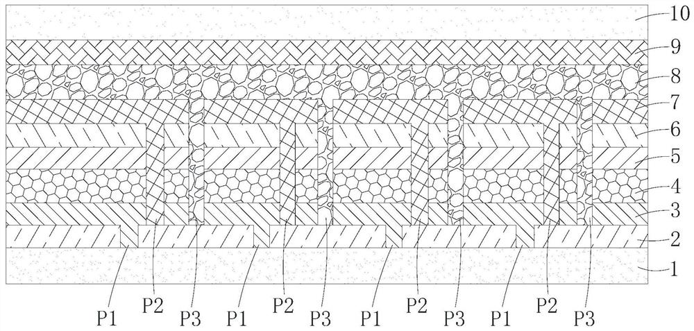
[0038] Step 11 , perform laser etching on the conductive glass substrate 1 on which the fluorine doped tin oxide (FTO) front conductive layer 2 is deposited, and etch away the FTO with a width of 50 μm, which is marked as a cutting line groove P1 . The conductive glass substrate 1 on which the conductive layer 2 before the FTO is deposited is cleaned, dried with nitrogen, and treated with ultraviolet and ozone.

[0039] Step 12, deposit TiO on the front conductive layer 2 2 The front carrier transport layer 3, the material of the front carrier transport layer 3 fills the cutting line groove P1, and the front carrier transport layer 3 includes a dense layer with a thickness of 20 nm and a mesoporous layer with a thickness of 100 nm. The substrate of the carrier transport layer 3 was heated to 70°C before deposition. The prepa...

Embodiment 2

[0047] The second embodiment of the packaging process of the perovskite optoelectronic component of the present invention includes the following steps:

[0048] Step 21 , perform laser etching on the conductive glass substrate 1 on which the indium doped tin oxide (ITO) front conductive layer 2 is deposited, and etch away the ITO with a width of 100 μm, which is denoted as a cutting line groove P1 . Then, the conductive glass substrate 1 on which the pre-ITO conductive layer 2 is deposited is cleaned, dried with nitrogen, and treated with ultraviolet and ozone.

[0049] Step 22 , spray a 20 nm NiOx front carrier transport layer 3 on the front conductive layer 2 , and the material of the front carrier transport layer 3 fills the cutting wire slot P1 . After drying, keep the temperature of substrate 1 at 70°C, spray 0.7mol / L lead iodide solution, and use N,N-dimethylformamide and dimethyl sulfoxide with a volume ratio of 9:1 as a mixed solvent, Annealed at 70 °C for 10 min to o...

Embodiment 3

[0057] The third embodiment of the packaging process of the perovskite optoelectronic component of the present invention includes the following steps:

[0058] Step 31 , perform laser etching on the conductive glass substrate 1 on which the indium doped tin oxide (ITO) front conductive layer 2 is deposited, and etch away the ITO with a width of 80 μm, which is marked as a cutting line groove P1 . Then, the conductive glass substrate 1 on which the pre-ITO conductive layer is deposited is cleaned, dried with nitrogen, and treated with ultraviolet and ozone.

[0059] Step 32: Coating poly[bis(4-phenyl)(2,4,6-trimethylphenyl)amine] (PTAA) with a thickness of 20 nm on the front conductive layer 2 as the front carrier transport layer 3, The material of the front carrier transport layer 3 fills the cutting wire slot P1. After drying, 1.2mol / L MAPbI 3 The methylamine acetic acid solution was coated on the surface of the front carrier transport layer 3 and annealed at 100° C. for 10...


PUM

PropertyMeasurementUnit
thicknessaaaaaaaaaa

Abstract

The invention relates to a perovskite photoelectric assembly which comprises a substrate, a front conducting layer, a front carrier transport layer, a perovskite light absorption layer, a rear carrier transport layer, a barrier layer, a back electrode layer, a protective layer, an adhesive film layer and an upper packaging glass layer from bottom to top in sequence, n-1 cutting line grooves P1 are formed in the front conducting layer, the P1 cut off the front conducting layer, n-1 cutting line grooves P2 are formed in the barrier layer, the P2 are located at the sides corresponding to the P1 respectively, the P2 cut off the barrier layer, the rear carrier transport layer, the perovskite light absorption layer and the front carrier transport layer at the same time, n-1 cutting line grooves P3 are formed in the back electrode layer, the P3 and the corresponding P2 are located in the same side, and the P3 cut off the back electrode layer, the barrier layer, the rear carrier transport layer, the perovskite light absorption layer and the front carrier transport layer at the same time. The invention further discloses a packaging process of the perovskite photoelectric assembly. According to the invention, the problem of easy occurrence of short circuit after assembly lamination is effectively solved, and the thermal stability of the perovskite assembly is improved.

Description

technical field [0001] The invention belongs to the technical field of preparation of perovskite optoelectronic components, and particularly relates to a perovskite optoelectronic component and a packaging process thereof. Background technique [0002] Existing perovskite devices used in industry are generally packaged large-area perovskite components. When packaging perovskite optoelectronic components, a common and convenient method is to place adhesive film and packaging glass on top of perovskite optoelectronic components. The assembly is then sealed through a lamination process. A lamination process is usually required, but the pressure applied to the assembly during lamination may cause the conductive material on top of the cell (such as metal electrodes, metal or metal oxide barrier layers) to come into direct contact through the laser-cut trenches The conductive substrate at the bottom of the module causes a short circuit, aggravates battery aging, and reduces batte...

Claims


Application Information

Patent Timeline
Patent Type & Authority Applications(China)
IPC IPC(8): H01L51/52H01L51/56
CPCH10K50/8426H10K71/00
Inventor 不公告发明人
Owner HANGZHOU MICROQUANTA SEMICON CO LTD
Why Eureka
Try Eureka