Method for manufacturing lower substrate of triple-medium layer of field emission display
A field emission and display technology, which is applied to the production of the insulating dielectric layer between the gate and the cathode and the gate, and the cathode field of the lower substrate, can solve the problems of poor insulation and short circuit of the cathode gate, and achieve the effect of improving the withstand voltage characteristics.
- Summary
- Abstract
- Description
- Claims
- Application Information
AI Technical Summary
Problems solved by technology
Method used
Image

Examples
Embodiment 1
[0018] A method for manufacturing a substrate under a triple dielectric layer of a field emission display, comprising the steps of:
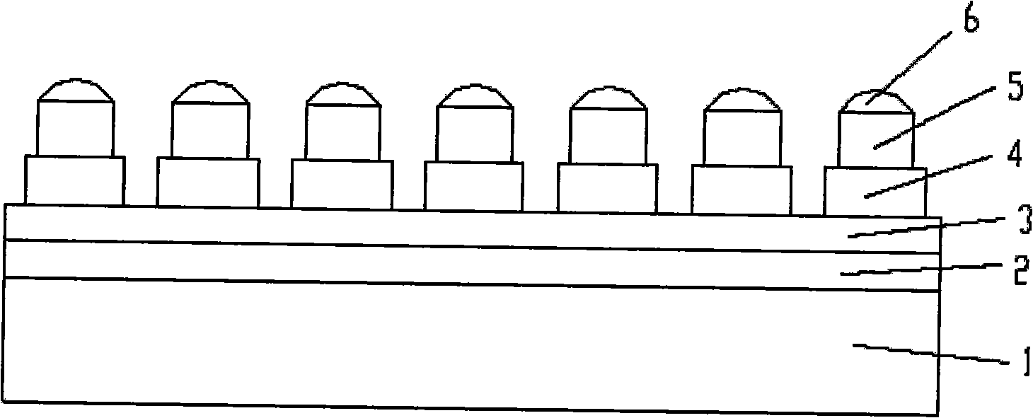
[0019] 1) On the glass substrate 1, use the electrode paste VG903 of DuPont to print the gate electrode layer 2 in sequence, and then use the prepared photosensitive medium paste to print the first photosensitive medium layer 3, and dry it at 100°C for 30 minutes to obtain the grid electrode. The thickness of the electrode layer 2 is 10 microns, and the thickness of the first photosensitive medium layer 3 is 30 microns;
[0020] 2) Cover the first photosensitive medium layer 3 and the gate electrode layer 2 with a grid mask plate, and perform one-time exposure and development on the first photosensitive medium layer 3 and the gate electrode layer 2. The exposure time is 12 minutes, and the wavelength of ultraviolet light is 360 nanometers, and then developed with 0.5% aqueous sodium carbonate solution to obtain grid line patterns;
[0021] 3) P...
Embodiment 2
[0028] A method for manufacturing a substrate under a triple dielectric layer of a field emission display, comprising the steps of:
[0029] 1) On the glass substrate 1, the electrode paste VG903 of DuPont Company was used to print the gate electrode layer 2 sequentially, and then the first photosensitive medium layer 3 was printed using the prepared photosensitive medium paste, and dried at 120° C. for 20 minutes to obtain the first The thickness of the photosensitive medium layer is 15 microns, and the thickness of the gate electrode layer 2 is 10 microns;
[0030] 2) Cover the first photosensitive medium layer 3 and the gate electrode layer 2 with a grid mask plate, and perform one-time exposure and development on the first photosensitive medium layer 3 and the gate electrode layer 2. The exposure time is 12 minutes, and the wavelength of ultraviolet light is 360 nanometers, and then developed with 0.5% aqueous sodium carbonate solution to obtain grid line patterns;
[003...
Embodiment 3
[0038] A method for manufacturing a substrate under a triple dielectric layer of a field emission display, comprising the steps of:
[0039] 1) On the glass substrate 1, use the electrode paste VG903 of DuPont to print the gate electrode layer 2 in sequence, and then use the prepared photosensitive medium paste to print the first photosensitive medium layer 3, and dry it at 130°C for 10 minutes to obtain the grid electrode. The thickness of the electrode layer 2 is 30 microns, and the thickness of the first photosensitive medium layer 3 is 20 microns;
[0040] 2) Cover the first photosensitive medium layer 3 and the gate electrode layer 2 with a gate mask plate, and perform one-time exposure and development on the first photosensitive medium layer 3 and the gate electrode layer 2. The exposure time is 12 minutes, and the wavelength of ultraviolet light is 360 nanometers, and then developed with 0.5% aqueous sodium carbonate solution to obtain grid line patterns;
[0041]3) Pr...
PUM
 Abstract
Description
Claims
Application Information
 - R&D
- Intellectual Property
- Life Sciences
- Materials
- Tech Scout
- Unparalleled Data Quality
- Higher Quality Content
- 60% Fewer Hallucinations
Browse by: Latest US Patents, China's latest patents, Technical Efficacy Thesaurus, Application Domain, Technology Topic, Popular Technical Reports.
© 2025 PatSnap. All rights reserved.Legal|Privacy policy|Modern Slavery Act Transparency Statement|Sitemap|About US| Contact US: help@patsnap.com