Array substrate, preparation method thereof and display panel
A technology for array substrates and substrates, applied in the field of array substrates and their preparation, can solve problems such as easy shorting of adjacent signal lines
- Summary
- Abstract
- Description
- Claims
- Application Information
AI Technical Summary
Problems solved by technology
Method used
Image

Examples
Embodiment 1
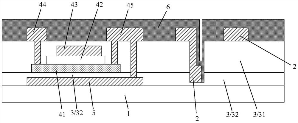
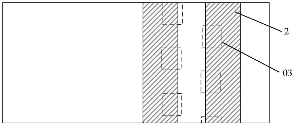
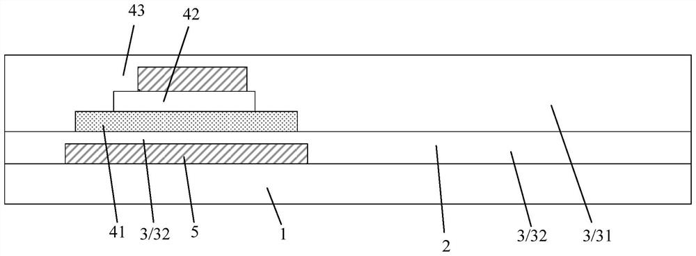
[0033] like figure 1 and figure 2 As shown, this embodiment provides an array substrate, including: a substrate 1 , a signal line 2 disposed on the substrate 1 , and an insulating layer 3 disposed on a layer where the signal line 2 is located close to the substrate 1 . In particular, in this embodiment, the insulating layer 3 has a groove; part of the edge of the signal line 2 falls into the groove.
[0034] In the array substrate provided in this embodiment, by setting grooves in the insulating layer 3, the grooves located above the insulating layer 3 ( figure 1 The edge of the signal line 2 on the side away from the substrate 1) falls into the groove, so that the distance between the signal line 2 in this part and other electronic components on the array substrate is increased in disguise, and the signal line 2 and other electronic components on the array substrate are avoided as far as possible. Defects occur between other electronic components due to too narrow spacing....
Embodiment 2
[0048] This embodiment provides a display panel, including any one of the array substrates provided in Embodiment 1.
[0049] Specifically, the display panel can be any product or component with a display function such as an organic light emitting diode (OLED) display panel, electronic paper, mobile phone, tablet computer, television, monitor, notebook computer, digital photo frame, and navigator.
Embodiment 3
[0051] like Figure 1 to Figure 5 As shown, this embodiment provides a method for preparing an array substrate, which can be used to prepare any of the array substrates provided in Embodiment 1. The preparation method may include the following steps:
[0052] S11, forming an insulating layer 3 on the substrate 1 through a patterning process; the insulating layer 3 has grooves.
[0053] In this step, an insulating layer 3 may be formed on the substrate 1, and then grooves are formed on the insulating layer 3 by an etching process. Wherein, the position of the groove corresponds to the signal line 2 to be formed later.
[0054] S12 , forming the signal line 2 on the substrate 1 formed with the insulating layer 3 , and part of the edge of the signal line 2 falls into the groove.
[0055] In this step, a conductive layer (such as a metal layer) may be formed on the substrate 1 first, and then the signal line 2 is formed by an etching process. For the position of the signal lin...
PUM
| Property | Measurement | Unit |
|---|---|---|
| Thickness | aaaaa | aaaaa |
| Thickness | aaaaa | aaaaa |
| Thickness | aaaaa | aaaaa |
Abstract
Description
Claims
Application Information
 - R&D
- Intellectual Property
- Life Sciences
- Materials
- Tech Scout
- Unparalleled Data Quality
- Higher Quality Content
- 60% Fewer Hallucinations
Browse by: Latest US Patents, China's latest patents, Technical Efficacy Thesaurus, Application Domain, Technology Topic, Popular Technical Reports.
© 2025 PatSnap. All rights reserved.Legal|Privacy policy|Modern Slavery Act Transparency Statement|Sitemap|About US| Contact US: help@patsnap.com