
Semiconductor integrated circuit device

A technology of integrated circuits and semiconductors, applied in the manufacture of semiconductor devices, circuits, and semiconductor/solid-state devices, etc., can solve problems such as increased power consumption, and achieve the effect of improving yield and suppressing manufacturing and performance.

Pending Publication Date: 2021-07-30
SOCIONEXT INC
View PDF0 Cites 0 Cited by
  • Summary
  • Abstract
  • Description
  • Claims
  • Application Information

AI Technical Summary

Problems solved by technology

However, in recent years, there has been a problem that excessive scaling down causes off-current, which in turn causes a significant increase in power consumption

Method used


Image

  • Semiconductor integrated circuit device
  • Semiconductor integrated circuit device
  • Semiconductor integrated circuit device

Examples


no. 1 approach

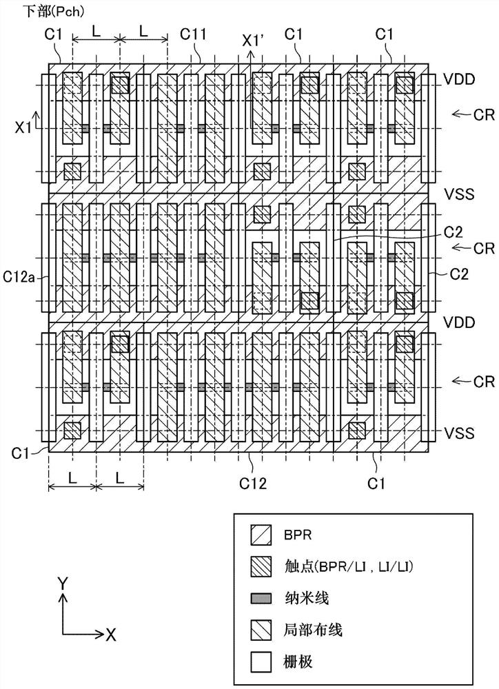
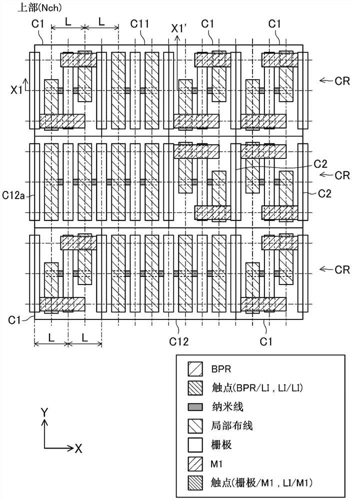
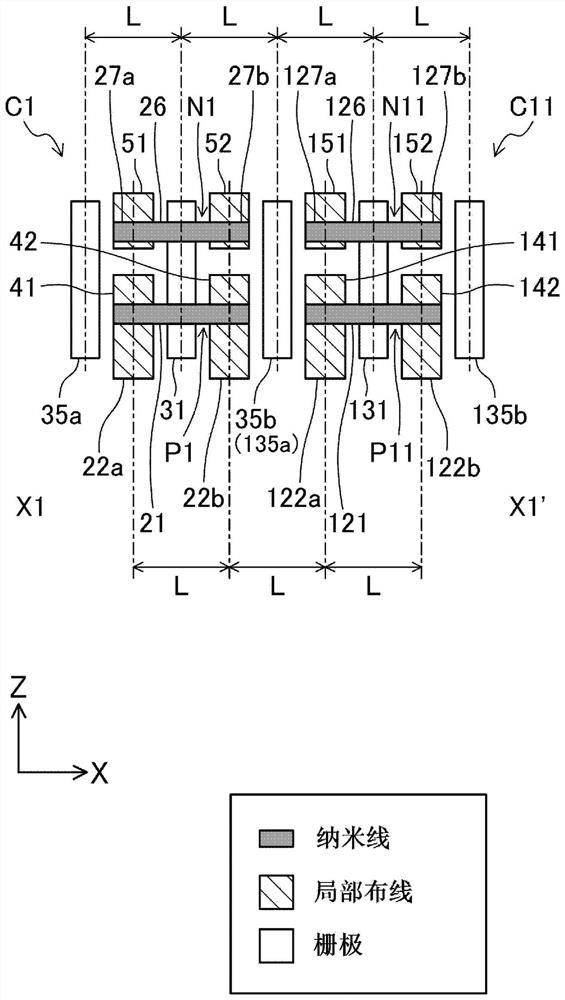
[0052] figure 1 is an example of the layout of the lower part of the circuit block using the standard cell according to the first embodiment, figure 2 is an example of the layout of the upper part of the circuit block using the standard cell according to the first embodiment, image 3 is along figure 1 and figure 2 The section cut by the line X1-X1'. figure 1 and figure 2 is a top view of the circuit block. in particular, figure 1 The lower part is shown, that is, the part including the three-dimensional structure transistor (here, a P-type nanowire FET) formed on the side close to the substrate, figure 2 The upper part is shown, that is, the part including the three-dimensional structure transistor (here, N-type nanowire FET) formed on the side away from the substrate.

[0053] It should be noted that, in the following description, in figure 1 In the top view, the horizontal direction of the drawing is defined as the X direction (corresponding to the first directi...

no. 2 approach

[0134] Figure 12 is a diagram showing the layout structure of the filling cell according to the second embodiment, Figure 12 (a) shows the lower part of the unit, Figure 12 (b) shows the upper part of the unit. The filling cell C21 has no P-type or N-type dummy transistors.

[0135] Such as Figure 12 As shown in (a), power supply wirings 211 and 212 extending in the X direction are respectively provided at both ends of the filling cell C21 in the Y direction. Both the power supply wirings 211 and 212 are buried power supply wirings (BPR) formed in the buried wiring layer. The power supply wiring 211 is supplied with the same power supply voltage VDD as that of the power supply wiring 11 . The power supply wiring 212 supplies the same power supply voltage VSS as that of the power supply wiring 12 .

[0136] In the filling cell C21 , a dummy gate wiring 231 extending in the Y direction substantially at the center in the X direction and extending in the Z direction from...


PUM


Abstract

An inverter cell (C1) having a logic function and a filler cell (C11) having no logic function are disposed adjacent to each other. Nanowires (122,126) of the filler cell (C11) are respectively disposed at the same locations as nanowires (22,26) of the inverter cell (C1) in a Y-direction. A P-type dummy transistor (P11) and an N-type dummy transistor (N11) of the filler cell (C11) are respectively disposed in the same layers as a P-type transistor (P1) and an N-type transistor (N1) in a Z-direction.

Description

technical field [0001] The present disclosure relates to a semiconductor integrated circuit device including a standard cell (hereinafter also simply referred to as a cell as the case may be) including a three-dimensional structure transistor. Background technique [0002] The standard cell approach is a known method of forming semiconductor integrated circuits on a semiconductor substrate. The standard cell method refers to the following method, that is, the basic cells with specific logic functions (such as inverters, latches, flip-flops, full adders, etc.) are prepared as standard cells in advance, and then multiple standard cells are arranged On the semiconductor substrate, these standard cells are connected by wiring, so as to design the LSI chip. [0003] Transistors, which are the basic constituent elements of LSI, have achieved increased integration, reduced operating voltage, and improved operating speed by reducing the gate length (scaling). However, in recent ye...

Claims


Application Information

Patent Timeline
Patent Type & Authority Applications(China)
IPC IPC(8): H01L21/82H01L21/822H01L27/04H01L21/8234H01L27/088H01L21/8238H01L27/092H01L29/06
CPCH01L27/092H01L27/0207H01L21/76895H01L23/5286H01L23/535H01L23/5222H01L29/0673H01L29/42392H01L29/78696
Inventor 伊达浩志郎
Owner SOCIONEXT INC
Learn More