Single crystal battery and preparation method thereof
A single crystal and battery technology, applied in the manufacture of circuits, electrical components, final products, etc., can solve problems such as low power efficiency, poor potential-induced attenuation effect, and poor light-induced attenuation effect
- Summary
- Abstract
- Description
- Claims
- Application Information
AI Technical Summary
Problems solved by technology
Method used
Image

Examples
Embodiment 1
[0077] In this example, a monocrystalline battery is prepared according to the following method:
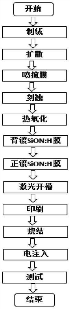
[0078] a) 10,000 pieces of silicon wafers of the single crystal M2 type are used, and the silicon wafers are etched with alkaline solution to make suede;
[0079] b) Put the textured silicon wafer into the low-pressure diffusion furnace equipment, pass the phosphorus source to make a PN junction, and control the square resistance to 70Ω;
[0080] c) Spray a paraffin mask on a part of the surface of the silicon wafer using mask spraying equipment, and the pattern of this mask is consistent with the pattern of the metal grid lines printed on the front side of the subsequent silicon wafer;
[0081] d) In the chain-type acid polishing and etching equipment, spray the masked silicon wafer in some areas of step c), first use hydrofluoric acid to remove the PN junction around the silicon wafer and the back side, and then soak the silicon wafer in hydrofluoric acid and Remove the oxide ...
Embodiment 2
[0093] In this example, a monocrystalline battery is prepared according to the following method:
[0094] a) 10,000 pieces of silicon wafers of the single crystal M2 type are used, and the silicon wafers are etched with alkaline solution to make suede;
[0095] b) Put the textured silicon wafer into the low-pressure diffusion furnace equipment, pass the phosphorus source to make a PN junction, and control the square resistance at 75Ω;
[0096] c) Spray a paraffin mask on a part of the surface of the silicon wafer using mask spraying equipment, and the pattern of this mask is consistent with the pattern of the metal grid lines printed on the front side of the subsequent silicon wafer;
[0097] d) In the chain-type acid polishing and etching equipment, spray the masked silicon wafer in some areas of step c), first use hydrofluoric acid to remove the PN junction around the silicon wafer and the back side, and then soak the silicon wafer in hydrofluoric acid and Remove the oxide ...
Embodiment 3
[0108] In this example, a monocrystalline battery is prepared according to the following method:
[0109] a) 10,000 pieces of silicon wafers of the single crystal M2 type are used, and the silicon wafers are etched with alkaline solution to make suede;
[0110] b) Put the textured silicon wafer into the low-pressure diffusion furnace equipment, pass the phosphorus source to make a PN junction, and control the square resistance at 80Ω;
[0111] c) Spray a paraffin mask on a part of the surface of the silicon wafer using mask spraying equipment, and the pattern of this mask is consistent with the pattern of the metal grid lines printed on the front side of the subsequent silicon wafer;
[0112] d) In the chain-type acid polishing and etching equipment, spray the masked silicon wafer in some areas of step c), first use hydrofluoric acid to remove the PN junction around the silicon wafer and the back side, and then soak the silicon wafer in hydrofluoric acid and Remove the oxide ...
PUM
| Property | Measurement | Unit |
|---|---|---|
| Square resistance | aaaaa | aaaaa |
| Thickness | aaaaa | aaaaa |
| Thickness | aaaaa | aaaaa |
Abstract
Description
Claims
Application Information
 - R&D
- Intellectual Property
- Life Sciences
- Materials
- Tech Scout
- Unparalleled Data Quality
- Higher Quality Content
- 60% Fewer Hallucinations
Browse by: Latest US Patents, China's latest patents, Technical Efficacy Thesaurus, Application Domain, Technology Topic, Popular Technical Reports.
© 2025 PatSnap. All rights reserved.Legal|Privacy policy|Modern Slavery Act Transparency Statement|Sitemap|About US| Contact US: help@patsnap.com