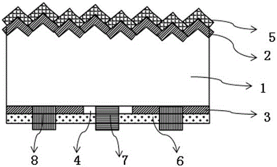
A kind of manufacturing method of n-type IBC silicon solar cell based on ion implantation process
A silicon solar cell and ion implantation technology, applied in the field of solar cells, can solve problems such as low boron content, and achieve the effects of high minority carrier lifetime, technical precision, and reduced recombination rate
- Summary
- Abstract
- Description
- Claims
- Application Information
AI Technical Summary
Problems solved by technology
Method used
Image
Examples
Embodiment 1
[0036] This embodiment includes the following steps:
[0037] 1. Select an n-type silicon substrate with a resistivity of 3-5Ω·cm, and its minority carrier lifetime is greater than 500us, use chemical etching to remove the damaged layer on the surface of the silicon wafer, and make texture on both sides.
[0038] 2. Double-sided phosphorus diffusion: the diffusion resistance is 60Ω / □.
[0039] 3. Print corrosive paste on the p+ defined area on the back to remove the phosphosilicate glass in the p+ defined area.
[0040] 4. Use 20% TMAH solution to carry out selective etching at 60°C, polish the p+ defined area, and etch for 30 minutes.
[0041] 5. Remove the phosphosilicate glass on the front surface of the n-type silicon substrate, and use hydrofluoric acid, nitric acid and water with a volume ratio of 1:30:300 to etch the front surface of the n-type silicon substrate. 140Ω / □.
[0042] 6. Remove the back phosphosilicate glass and perform RCA cleaning.
[0043] 7. Using th...
Embodiment 2
[0050] This embodiment includes the following steps:
[0051] 1. Select an N-type silicon substrate with a resistivity of 5-12Ω·cm, whose minority carrier lifetime is greater than 500us, remove the damaged layer on the surface of the silicon wafer by chemical etching, and make texture on both sides.
[0052] 2. Double-sided phosphorus diffusion: the diffusion resistance is 80Ω / □.
[0053] 3. Use laser to remove the phosphosilicate glass in the p+ defined area.
[0054]4. Use 25% TMAH solution to carry out selective etching at 70°C, and polish the p+ defined area, and the etching time is 20 minutes.
[0055] 5. Remove the phosphosilicate glass on the front surface of the n-type silicon substrate, use 1:30:300 hydrofluoric acid, nitric acid and water to etch the front surface of the n-type silicon substrate at 25°C, and the etching time is 20min. The square resistance of the front surface after etching was 130Ω / □.
[0056] 6. Remove the back phosphosilicate glass and perform ...
PUM
 Abstract
Description
Claims
Application Information
 - R&D
- Intellectual Property
- Life Sciences
- Materials
- Tech Scout
- Unparalleled Data Quality
- Higher Quality Content
- 60% Fewer Hallucinations
Browse by: Latest US Patents, China's latest patents, Technical Efficacy Thesaurus, Application Domain, Technology Topic, Popular Technical Reports.
© 2025 PatSnap. All rights reserved.Legal|Privacy policy|Modern Slavery Act Transparency Statement|Sitemap|About US| Contact US: help@patsnap.com

