Processing device
A processing device and transportation device technology, applied in sustainable manufacturing/processing, electrical components, climate sustainability, etc., can solve problems such as increased process cost, poor resistance uniformity, and poor electrical properties
- Summary
- Abstract
- Description
- Claims
- Application Information
AI Technical Summary
Problems solved by technology
Method used
Image

Examples
Embodiment Construction
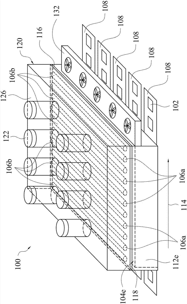
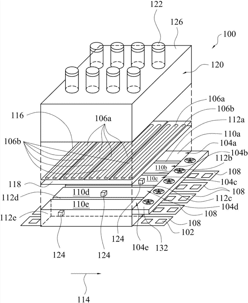
[0022] In order to improve the light-induced attenuation phenomenon of semiconductor solar cells, there is currently a method of performing light-heating treatment on semiconductor solar cells. In this way, many light sources are arranged above the multi-channel transmission device in the chamber of the processing device. When the semiconductor solar cells are transported in the chamber through the transmission device, the light sources can perform light and heat treatment on the semiconductor solar cells to eliminate the semiconductor solar cells. cell defects, thereby improving the light-induced degradation of semiconductor solar cells.
[0023] However, in order to provide sufficient illuminance for semiconductor solar cells in this way, most of them use halogen lamps as light sources, which will generate excessive heat and cause the temperature in the chamber of the processing device to be too high. When the temperature in the chamber is too high, it is impossible to direc...
PUM
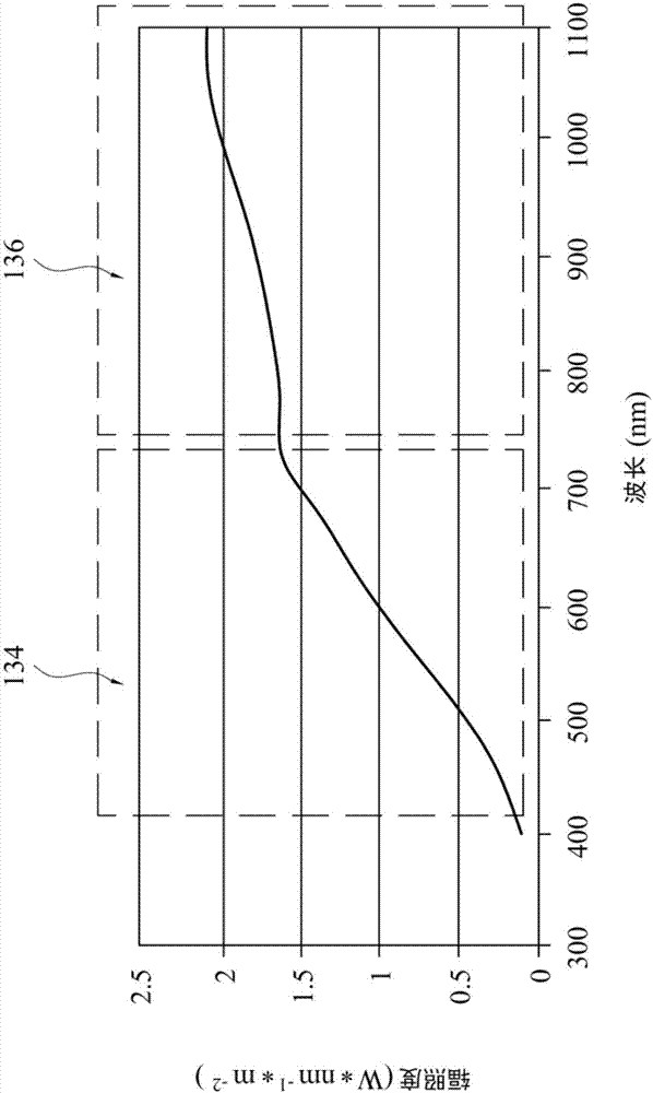
| Property | Measurement | Unit |
|---|---|---|
| Peak wavelength | aaaaa | aaaaa |
| Peak wavelength | aaaaa | aaaaa |
Abstract
Description
Claims
Application Information
 - R&D
- Intellectual Property
- Life Sciences
- Materials
- Tech Scout
- Unparalleled Data Quality
- Higher Quality Content
- 60% Fewer Hallucinations
Browse by: Latest US Patents, China's latest patents, Technical Efficacy Thesaurus, Application Domain, Technology Topic, Popular Technical Reports.
© 2025 PatSnap. All rights reserved.Legal|Privacy policy|Modern Slavery Act Transparency Statement|Sitemap|About US| Contact US: help@patsnap.com