Semiconductor HEMT device and manufacturing method thereof

A manufacturing method and semiconductor technology, applied in semiconductor/solid-state device manufacturing, semiconductor devices, semiconductor/solid-state device components, etc., can solve problems such as device cracking, lattice mismatch and thermal mismatch, and achieve not easy to fall off and reduce stress Concentrated, easy-off effect

Active Publication Date: 2021-07-09
深圳市红与蓝企业管理中心(有限合伙)
View PDF10 Cites 0 Cited by
  • Summary
  • Abstract
  • Description
  • Claims
  • Application Information

AI Technical Summary

Problems solved by technology

The substrates of HEMT devices in the prior art are all prepared based on silicon, sapphire, and silicon carbide materials, but when these materials are used as the substrate substrate, there will be a large lattice mismatch and thermal mismatch with the insulating layer, and it is easy to Device cracking due to stress concentration

Method used


Image

  • Semiconductor HEMT device and manufacturing method thereof
  • Semiconductor HEMT device and manufacturing method thereof
  • Semiconductor HEMT device and manufacturing method thereof

Examples


Embodiment 1

[0038] refer to Figure 9 , the present embodiment provides a semiconductor HEMT device, comprising:

[0039] Substrate Substrate 1.

[0040] The heat conduction layer, the heat conduction layer is located on the surface of one side of the base substrate 1 .

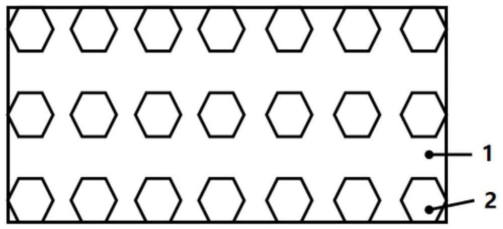
[0041] The heat conduction layer includes: a plurality of support structures 2 and heat conduction structures 3 arranged at intervals, the support structure 2 is located on one side surface of the base substrate 1; the heat conduction structure 3 is located on the surface of the base substrate 1 on the same side as the support structure 2, and the heat conduction structure 3 filling the gaps between the plurality of support structures 2.

[0042] The insulating layer 4 covers the surface of the heat conducting structure 3 facing away from the base substrate 1 , and the insulating layer 4 also covers the surfaces of the plurality of support structures 2 facing away from the base substrate 1 .

[0043] Wherein, the heat...

Embodiment 2

[0059] refer to Figure 2-Figure 9 , the present embodiment provides a method for manufacturing a semiconductor HEMT device, comprising the following steps:

[0060] providing a base substrate 1;

[0061] refer to Figure 2-Figure 5 , forming a heat conduction layer, the step of forming a heat conduction layer includes: forming a plurality of support structures 2 at intervals on one side surface of the base substrate 1; and then forming a heat conduction structure 3 on the side surface of the support structure 2 formed on the base substrate 1 , the heat conducting structure 3 fills the gaps between the plurality of supporting structures 2 .

[0062] An insulating layer 4 is formed, and the insulating layer 4 covers the surface of the thermally conductive structure 3 facing away from the base substrate 1 , and the insulating layer 4 also covers the surfaces of the plurality of support structures 2 facing away from the base substrate 1 .

[0063] The heat conducting structure...


PUM

PropertyMeasurementUnit
heightaaaaaaaaaa
heightaaaaaaaaaa
heightaaaaaaaaaa

Abstract

The invention provides a semiconductor HEMT device and a manufacturing method thereof. The semiconductor HEMT device comprises: a substrate; a heat conduction layer which is located on the surface of one side of the substrate, and comprises a plurality of supporting structures arranged at intervals and a heat conduction structure, wherein the supporting structures are located on the surface of one side of the substrate; the heat conduction structure is located on the surface, on the same side as the supporting structures, of the substrate, and gaps among the multiple supporting structures are filled with the heat conduction structure; and an insulating layer which covers the surface of the side, back to the substrate, of the heat conduction structure, and further covers the surfaces of the sides, back to the substrate, of the multiple supporting structures, wherein the heat conduction structure is a carbon film. According to the semiconductor HEMT device, through the arrangement of the heat conduction layer, stress concentration caused by thermal mismatch of the device can be reduced, and the possibility of cracking of the device is reduced.

Description

technical field [0001] The invention relates to the technical field of thermal stability of semiconductor devices, in particular to a semiconductor HEMT device and a manufacturing method thereof. Background technique [0002] HEMT (High Electron Mobility Transistor), a high electron mobility transistor, is a heterojunction field effect transistor, also known as modulation doped field effect transistor (MODFET), two-dimensional electron gas field effect transistor (2-DEGFET), Selectively doped heterojunction transistors (SDHT), etc. HEMT devices and their integrated circuits can work in ultra-high frequency (millimeter wave) and ultra-high-speed fields. The substrates of HEMT devices in the prior art are all based on silicon, sapphire, and silicon carbide materials, but when these materials are used as the substrate substrate, there will be a large lattice mismatch and thermal mismatch with the insulating layer, and it is easy to The device cracks due to stress concentratio...

Claims


Application Information

Patent Timeline
Patent Type & Authority Applications(China)
IPC IPC(8): H01L23/373H01L23/00H01L29/778H01L21/335B82Y40/00
CPCH01L29/778H01L29/66462H01L23/562H01L23/3735H01L23/373B82Y40/00
Inventor 刘新科林峰陈勇利健黎晓华贺威
Owner 深圳市红与蓝企业管理中心(有限合伙)
Why Eureka
Try Eureka