Chemical method for preparing CuBiI4 photoelectric thin film material through wet-process elementary substance powder room-temperature reaction
A chemical method and photoelectric thin film technology, applied in the field of material chemistry, can solve problems such as limited application and industrialized mass production, large film band gap, difficult to preserve, etc., and achieve broad industrial application prospects, simple device and operation, and easy preservation Effect
- Summary
- Abstract
- Description
- Claims
- Application Information
AI Technical Summary
Problems solved by technology
Method used
Image
Examples
Embodiment 1
[0049]1. Preparatory work: Clean the ITO conductive glass with detergent and deionized water for 30 minutes, and then in ammonia water (25% by mass): hydrogen peroxide (30% by mass): ionized water with a volume ratio of 1:2: Cook in the mixed solution of 5 at 80°C for 30 minutes, and then use deionized water to sonicate for 30 minutes again. The treated ITO conductive glass is dried at 80°C, irradiated with ultraviolet light for half an hour, and stored in a clean desiccator for later use. use.
[0050] 2. Reaction steps: Weigh 0.0445g Cu powder, 0.1463g Bi powder (Cu:Bi molar ratio is 1:1), 0.3556g I 2 The pellets were placed in a 5mL amber glass vial with magnets. Stir for 20 hours to mix and react the three elemental substances, and then use a pipette to measure 900 μL of N,N dimethylformamide and 100 μL of glacial acetic acid and add them to the mixed powder to form a solution. Stirring was continued for 1 hour to fully react in solution.
[0051] 3. Post-treatment: Fil...
Embodiment 4
[0061] 1, preparatory work: as embodiment 1
[0062] 2. Reaction steps: Weigh 0.0178g Cu powder, 0.1463g Bi powder, 0.3023g I powder respectively 2 (Cu:Bi molar ratio is 0.4:1), put it into a 5mL brown glass sample bottle equipped with magnets, stir for 20 hours to mix and react the three elements, and then use a pipette to measure 850μL of N , N-dimethylformamide and 150 μL of glacial acetic acid were added to the mixed powder to form a solution. Stirring was continued for 1.5 hours to fully react in solution.
[0063] 3. Post-treatment: Filter the obtained solution with a polytetrafluoroethylene filter membrane, then spin-coat it on the treated ITO conductive glass, use the anti-solvent method to measure 240 μL of chlorobenzene with a pipette gun and spin-coat it on the film, and then Place it on a heating plate at 60-80°C and anneal for 5-10 minutes to get gray-black CuBiI 4 film. The XRD pattern of obtained sample sees Pic 4-1 , BiI was found from the XRD spectrum 3...
Embodiment 5
[0065] 1, preparatory work: as embodiment 1
[0066] 2. Reaction steps: Weigh 0.03558g Cu powder, 0.1463g Bi powder (Cu: Bi molar ratio is 0.8:1), 0.3378g I 2 Put them into a 5mL brown glass sample bottle with magnets, stir for 24 hours to mix and react the three elements, and then use a pipette gun to measure 850μL of N,N dimethylformamide and 150μL of glacial acetic acid Add to the mixed powder to form a solution. Stirring was continued for 2 hours to fully react in solution.
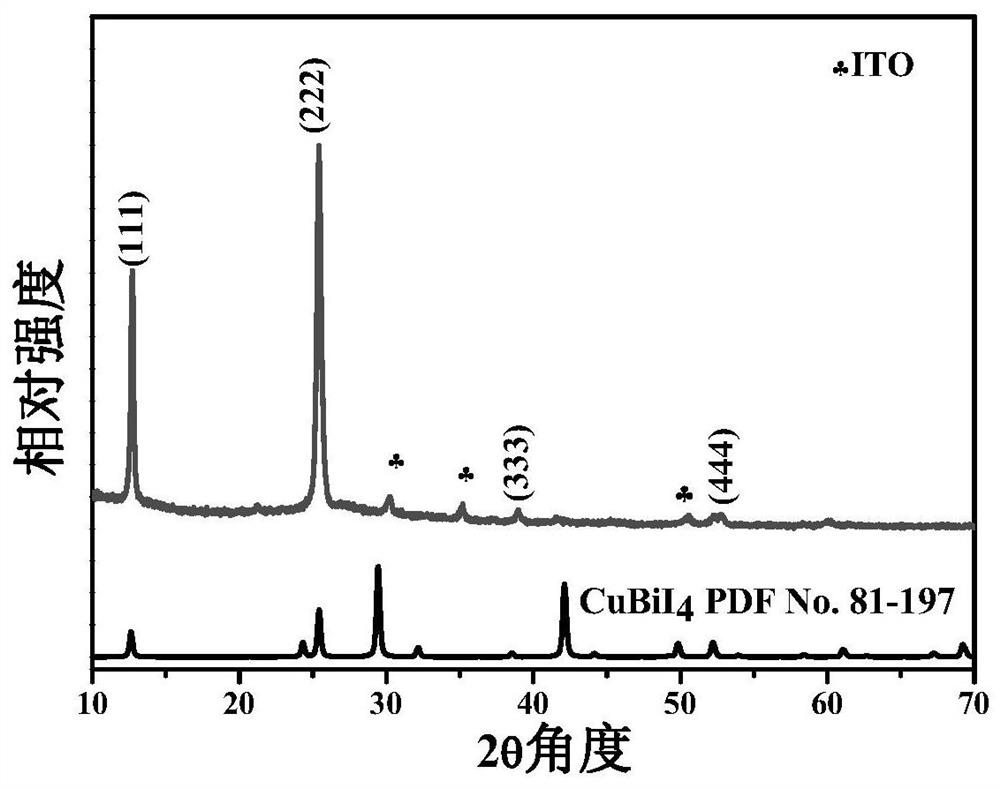
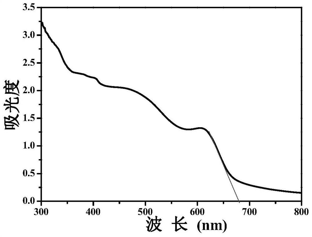
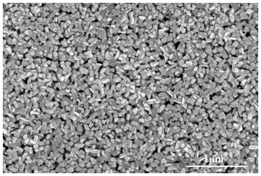
[0067] 3. Post-treatment: Filter the obtained solution with a polytetrafluoroethylene filter membrane, then spin-coat it on the treated ITO conductive glass, use the anti-solvent method to measure 240 μL of chlorobenzene with a pipette gun and spin-coat it on the film, and then Place it on a heating plate at 60-80°C and anneal for 5-10 minutes to get gray-black CuBiI 4 film. Figure 5-1 is the XRD pattern of the obtained sample, Figure 5-2 is its UV absorption curve, Figure 5-3 Transient surfa...
PUM
 Abstract
Description
Claims
Application Information
 - R&D
- Intellectual Property
- Life Sciences
- Materials
- Tech Scout
- Unparalleled Data Quality
- Higher Quality Content
- 60% Fewer Hallucinations
Browse by: Latest US Patents, China's latest patents, Technical Efficacy Thesaurus, Application Domain, Technology Topic, Popular Technical Reports.
© 2025 PatSnap. All rights reserved.Legal|Privacy policy|Modern Slavery Act Transparency Statement|Sitemap|About US| Contact US: help@patsnap.com


