A high-frequency and high-speed pcb board for macro and micro base stations for 5g communication and its preparation process
A kind of PCB board and preparation process technology, which is used in the manufacture of printed circuits, removal of conductive materials by chemical/electrolytic methods, and printed circuits. problems, to achieve the effects of improved etching accuracy, excellent high-speed/high-frequency transmission characteristics, and simple process
- Summary
- Abstract
- Description
- Claims
- Application Information
AI Technical Summary
Problems solved by technology
Method used
Image
Examples
Embodiment 1
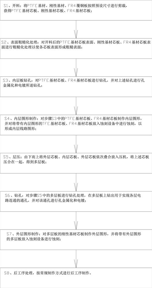
[0040] A preparation process of a macro / micro base station high-frequency and high-speed PCB board for 5G communication, comprising the following steps:
[0041] S1. Cutting: Cut the PTFE base material, rigid base material and FR4 copper clad laminate according to the preset size to obtain PTFE base material core board, rigid base material core board and FR4 base material core board;
[0042] S2. Surface roughening treatment: roughen the surface of the PTFE base material core plate, rigid base material core plate, and FR4 base material core plate after cutting to form a rough surface on the surface of each core plate; the surface roughening treatment The method is grinding plate or microetching.
[0043] S3. Inner plate drilling: Drill holes on PTFE substrate core boards and FR4 substrate core boards, and carry out hole metallization and electroplating on the above-mentioned drill holes; the hole metallization is ultrasonic copper sinking, and drilling Hole plating is pulse p...
Embodiment 2
[0050] A kind of preparation technology of macro / micro base station high-frequency high-speed PCB board for 5G communication, it is characterized in that comprising the following steps:
[0051] S1. Cutting: Cut the PTFE base material, rigid base material and FR4 copper clad laminate according to the preset size to obtain PTFE base material core board, rigid base material core board and FR4 base material core board;
[0052] S2. Surface roughening treatment: roughen the surface of the PTFE base material core plate, rigid base material core plate, and FR4 base material core plate after cutting to form a rough surface on the surface of each core plate; the surface roughening treatment The method is grinding plate or microetching.
[0053] S3. Inner plate drilling: Drill holes on PTFE substrate core boards and FR4 substrate core boards, and carry out hole metallization and electroplating on the above-mentioned drill holes; the hole metallization is ultrasonic copper sinking, and ...
Embodiment 3
[0060] A kind of preparation technology of macro / micro base station high-frequency high-speed PCB board for 5G communication, it is characterized in that comprising the following steps:
[0061] S1. Cutting: Cut the PTFE base material, rigid base material and FR4 copper clad laminate according to the preset size to obtain PTFE base material core board, rigid base material core board and FR4 base material core board;
[0062] S2. Surface roughening treatment: roughen the surface of the PTFE base material core plate, rigid base material core plate, and FR4 base material core plate after cutting to form a rough surface on the surface of each core plate; the surface roughening treatment The method is grinding plate or microetching.
[0063] S3. Inner plate drilling: Drill holes on PTFE substrate core boards and FR4 substrate core boards, and carry out hole metallization and electroplating on the above-mentioned drill holes; the hole metallization is ultrasonic copper sinking, and ...
PUM
 Abstract
Description
Claims
Application Information
 - R&D
- Intellectual Property
- Life Sciences
- Materials
- Tech Scout
- Unparalleled Data Quality
- Higher Quality Content
- 60% Fewer Hallucinations
Browse by: Latest US Patents, China's latest patents, Technical Efficacy Thesaurus, Application Domain, Technology Topic, Popular Technical Reports.
© 2025 PatSnap. All rights reserved.Legal|Privacy policy|Modern Slavery Act Transparency Statement|Sitemap|About US| Contact US: help@patsnap.com


