Preparation method of radiation-proof efficient gallium arsenide solar cell
A technology of solar cells and gallium arsenide, applied in the field of solar cells, can solve the problems of difficult to further improve the anti-radiation performance, slow progress, poor anti-irradiation performance, etc., to reduce the recombination probability, improve the absorption capacity, and improve the open circuit voltage. Effect
- Summary
- Abstract
- Description
- Claims
- Application Information
AI Technical Summary
Problems solved by technology
Method used
Image
Examples
preparation example Construction
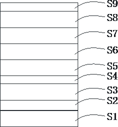
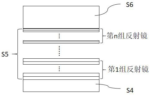
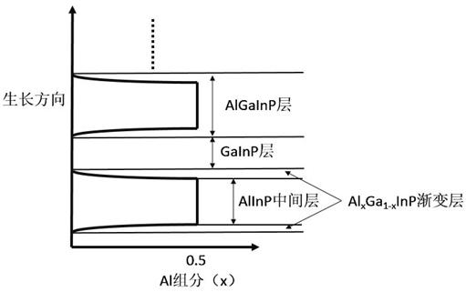
[0034] The following is attached Figure 1~3 This application will be described in detail. in, figure 1 Shown is a schematic structural diagram of the radiation-resistant high-efficiency gallium arsenide solar cell in this application. The solar cell consists of Ge substrate S1, bottom cell S2, buffer layer S3, mid-bottom tunnel junction S4, multi-reflector Center Bragg reflector S5, middle cell S6, middle top tunnel junction S7, top cell S8 and capping layer S9. The solar cell adopts multi-reflection center Bragg reflector technology to reflect back the light in the absorption band of the entire cell area to improve the solar cell. The absorption of incident sunlight by the region can further reduce the thickness of the battery region, reduce the reverse saturation current density, and improve the radiation resistance; use AlGaInP / GaInP material as the Bragg reflector material, and use the high radiation resistance of phosphide , to reduce the damage of the Bragg mirror mat...
Embodiment 1
[0053] A radiation-resistant high-efficiency gallium arsenide solar cell, from bottom to top are Ge substrate S1, bottom cell S2, buffer layer S3, middle bottom tunnel junction S4, multi-reflection center Bragg reflector S5, middle cell S6, middle cell The top tunnel junction S7, the top cell S8 and the capping layer S9. The specific production method is as follows:
[0054] (1) On a P-type Ge substrate, pass PH at high temperature 3 In the form of diffusion, the emitter area of the bottom cell S2 is formed, and then the GaInP nucleation layer is grown, and the nucleation layer serves as the window layer of the bottom cell S2 at the same time;
[0055] (2) Then grow GaAs buffer layer S3, the thickness of GaAs buffer layer S3 is 0.4 μm;
[0056] (3) Then grow the mid-bottom tunneling junction S4, and the mid-bottom tunneling junction S4 is N ++ GaAs / P ++ GaAs structure, where N ++ The thickness of GaAs is 0.02μm, and the doping concentration is 3×10 19 / cm 3 ;P ++ The...
PUM
| Property | Measurement | Unit |
|---|---|---|
| Thickness | aaaaa | aaaaa |
| Thickness | aaaaa | aaaaa |
| Thickness | aaaaa | aaaaa |
Abstract
Description
Claims
Application Information
 - R&D
- Intellectual Property
- Life Sciences
- Materials
- Tech Scout
- Unparalleled Data Quality
- Higher Quality Content
- 60% Fewer Hallucinations
Browse by: Latest US Patents, China's latest patents, Technical Efficacy Thesaurus, Application Domain, Technology Topic, Popular Technical Reports.
© 2025 PatSnap. All rights reserved.Legal|Privacy policy|Modern Slavery Act Transparency Statement|Sitemap|About US| Contact US: help@patsnap.com


