A kind of buffer layer growth method of silicon carbide epitaxial material

A technology of epitaxial materials and growth methods, which is applied in the field of buffer layer growth of epitaxial materials, can solve the problems of unstable C/Si ratio, increased defects, and low doping efficiency of buffer layers, so as to avoid unstable C/Si ratio, Alleviating large doping differences and improving doping efficiency

Active Publication Date: 2022-07-29
NO 55 INST CHINA ELECTRONIC SCI & TECHNOLOGYGROUP CO LTD
View PDF0 Cites 0 Cited by
  • Summary
  • Abstract
  • Description
  • Claims
  • Application Information

AI Technical Summary

Problems solved by technology

However, with the increase in the thickness of the epitaxial layer and the complexity of the multilayer structure, the defects in the epitaxial layer will also increase, which will greatly affect the semiconductor performance in terms of withstand voltage and mobility, and ultimately affect the finished product of the power semiconductor device. Serious impact on rate and performance
The substrate for SiC epitaxial materials is generally an off-axis substrate, and the SiC substrate itself has crystal defects during the growth process, and off-axis cutting is also easy to introduce new defects.
During the epitaxial growth process, substrate surface defects will extend to the epitaxial layer and be easily amplified, directly affecting the performance of chips and devices
However, the epitaxial layer (drift layer) of the existing power electronic devices is a low-doped thick-layer epitaxial material, which adopts a high-speed epitaxial process with a high C / Si ratio at the inlet end, which is prone to unstable C / Si ratio and doping in the buffer layer. The case of low efficiency

Method used


Image

  • A kind of buffer layer growth method of silicon carbide epitaxial material
  • A kind of buffer layer growth method of silicon carbide epitaxial material
  • A kind of buffer layer growth method of silicon carbide epitaxial material

Examples


Embodiment Construction

[0033] The present invention will be further described in detail below with reference to the accompanying drawings and specific embodiments.

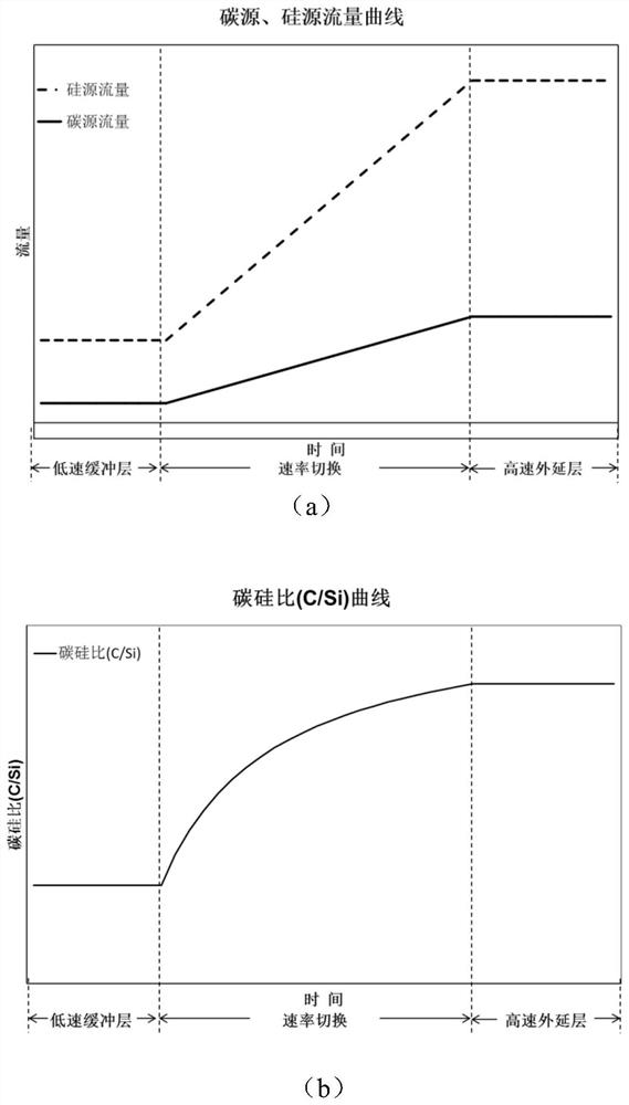
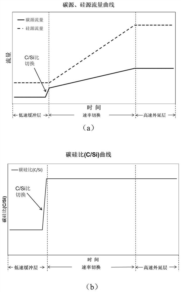
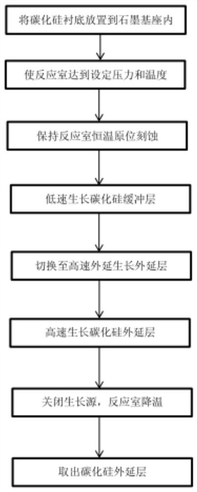
[0034] In order to reduce the influence of the substrate on the epitaxial layer, a buffer layer process is added to the epitaxial process. On the one hand, the buffer layer can reduce the stress and defects caused by the difference in doping concentration between the substrate and the epitaxial layer, and on the other hand, it can also effectively It can effectively suppress the extension and amplification of substrate defects into the epitaxial layer, thereby effectively improving the quality of epitaxial materials and ensuring the performance of chips and devices. To ensure the effect of the buffer layer, the buffer layer of the present invention adopts a low-speed epitaxy process with a low carbon-to-silicon ratio (C / Si ratio) at the gas inlet. figure 1 (a) is the flow adjustment curve of the carbon source and silicon source during t...


PUM

PropertyMeasurementUnit
thicknessaaaaaaaaaa
thicknessaaaaaaaaaa

Abstract

The invention discloses a buffer layer growth method of silicon carbide epitaxial material, which adopts low-high C / Si ratio switching at the end of low-speed buffer layer growth, and quickly completes the switching in a short time, so as to increase the C / Si ratio more quickly. . By adopting an optimized process switching process between the buffer layer and the epitaxial layer, the present invention realizes that the carbon-to-silicon ratio (C / Si) remains stable over time during the switching process between the growth of the low-speed buffer layer and the growth of the high-speed epitaxial layer. The carbon source flow rate and the silicon source flow rate are both very low, and a relatively small increase in the carbon source flow rate can meet the requirements for improving the C / Si ratio, reduce the defects and stress introduced by the low-speed to high-speed rate switching process, and reduce the defects of epitaxial materials. Density to achieve high-quality SiC epitaxial material growth.

Description

technical field [0001] The invention relates to a buffer layer growth method of epitaxial material, in particular to a buffer layer growth method of silicon carbide epitaxial material. Background technique [0002] At present, the third-generation wide-bandgap semiconductor material represented by silicon carbide (SiC) has the advantages of wide band gap, high thermal conductivity, high breakdown strength, high electron saturation drift speed, high hardness, etc., and also has strong chemical The stability makes silicon carbide have many advantages in applications, especially suitable for high power, high temperature and high frequency applications. [0003] The SiC device structure must be realized by epitaxy, and the performance advantage of SiC material is particularly significant at high voltage, so thick-layer homoepitaxial growth is required. However, with the increase in the thickness of the epitaxial layer and the complication of the multi-layer structure, the defec...

Claims


Application Information

Patent Timeline
Patent Type & Authority Patents(China)
IPC IPC(8): H01L21/02H01L21/04H01L21/67
Inventor 周平李赟熊瑞王翼赵志飞李忠辉
Owner NO 55 INST CHINA ELECTRONIC SCI & TECHNOLOGYGROUP CO LTD
Why Eureka
Try Eureka