Horizontal homojunction bipolar transistor and preparation method thereof
A bipolar transistor and homojunction technology, applied in the field of microelectronics, can solve the problem of low amplification factor, achieve high common emitter amplification factor, high amplification factor, and fewer types of materials
- Summary
- Abstract
- Description
- Claims
- Application Information
AI Technical Summary
Problems solved by technology
Method used
Image

Examples
preparation example Construction
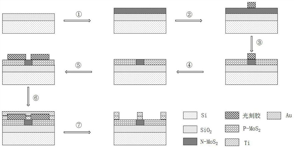
[0040] In the second aspect, the present invention provides a method for preparing the above-mentioned horizontal homojunction bipolar transistor, and the corresponding process flow chart is as follows figure 2 shown, including the following steps:
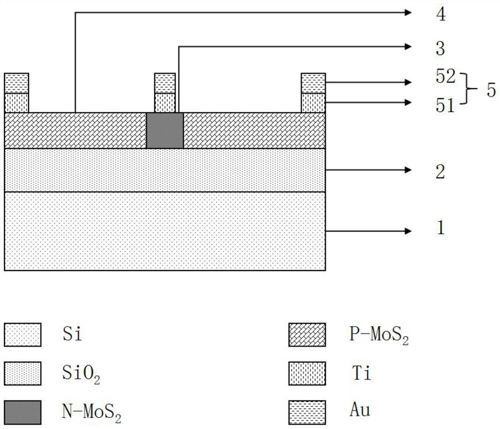
[0041] S1. Select SiO on the upper surface 2 Oxide layer of P-type doped single crystal silicon as the substrate, in SiO 2 Preparation of N-type MoS on oxide layer 2 Thin film, obtains first sample;
[0042] Specifically, in this embodiment, there will be SiO on the surface 2 P-type doped single crystal silicon (thickness: 350 μm) with an oxide layer (thickness: 50 nm) was used as a substrate, and acetone was used to sonicate it for 5 minutes to remove organic impurities on its surface. Sonicate it with ethanol for 5 min to remove the acetone on its surface. Then it was ultrasonicated with deionized water for 5 min to remove the ethanol on its surface. Finally, use a nitrogen gun to remove the deionized water on its surface...
Embodiment 1
[0056] A method for preparing a horizontal homojunction bipolar transistor, comprising the following steps:
[0057] S1. Select SiO on the upper surface 2 Oxide layer of P-type doped single crystal silicon as the substrate, in SiO 2 Preparation of N-type MoS on oxide layer 2 Thin film, obtains first sample;
[0058] S2. Perform the first ultraviolet lithography on the surface of the first sample, and after development, part of the N-type MoS is obtained 2 Thin film exposed, part of N-type MoS 2 A second sample with the film covered by photoresist;
[0059] S3. Doping the obtained second sample by low-energy ion implantation method, and obtaining the third sample after degelling;
[0060] S4. Carry out the second UV lithography on the surface of the third sample, and after developing, part of the area is obtained as N-type MoS 2 Thin film, part of the area is P-type MoS 2 a fourth sample of film;
[0061] S5. Evaporating metal on the surface of the obtained fourth sampl...
Embodiment 2
[0064] A method for preparing a horizontal homojunction bipolar transistor, comprising the following steps:
[0065] S1. Select SiO on the upper surface 2 Oxide layer of P-type doped single crystal silicon as the substrate, in SiO 2 Preparation of N-type MoS on oxide layer 2 Thin film, obtains first sample;
[0066] S2. Perform the first ultraviolet lithography on the surface of the first sample, and after development, part of the N-type MoS is obtained 2 Thin film exposed, part of N-type MoS 2 A second sample with the film covered by photoresist;
[0067] S3. Doping the obtained second sample by low-energy ion implantation method, and obtaining the third sample after degelling;
[0068] S4. Carry out the second UV lithography on the surface of the third sample, and after developing, part of the area is obtained as N-type MoS 2 Thin film, part of the area is P-type MoS 2 a fourth sample of film;
[0069] S5. Evaporating metal on the surface of the obtained fourth sampl...
PUM
| Property | Measurement | Unit |
|---|---|---|
| Thickness | aaaaa | aaaaa |
| Thickness | aaaaa | aaaaa |
| Thickness | aaaaa | aaaaa |
Abstract
Description
Claims
Application Information
 - R&D
- Intellectual Property
- Life Sciences
- Materials
- Tech Scout
- Unparalleled Data Quality
- Higher Quality Content
- 60% Fewer Hallucinations
Browse by: Latest US Patents, China's latest patents, Technical Efficacy Thesaurus, Application Domain, Technology Topic, Popular Technical Reports.
© 2025 PatSnap. All rights reserved.Legal|Privacy policy|Modern Slavery Act Transparency Statement|Sitemap|About US| Contact US: help@patsnap.com