


Quick Research
Generate reliable direction feasibility study reports for your R&D in just a few steps.

Technical Q&A
Discover and master advanced knowledge NOW. Basics, ideas, possibilities, all at once.

Find Solutions
As an expert in R&D theories, this can generate solutions to your technical problems instantly.

Evaluate Feasibility
Analyze your overall solution with one click, know your potential R&D risks in advance.

Monitor Landscape
Get weekly tech updates, stay abreast of the latest tech innovations and key insights.
Organic compound, electron transport material and application thereof
An organic compound and selected technology, applied in the field of organic compounds and electron transport materials, can solve the problems of affecting the luminous efficiency and stability of devices, imbalance of electron and hole mobility, poor carrier transport balance, etc. Electron flow, reduced exciton blocking, favorable balance effects
- Summary
- Abstract
- Description
- Claims
- Application Information
AI Technical Summary
Problems solved by technology
Method used
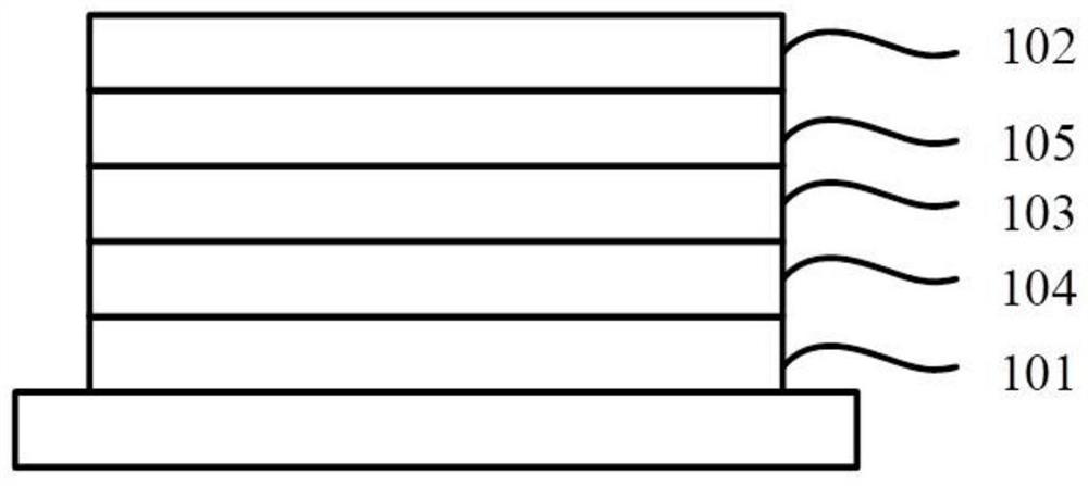
Image

Examples
Embodiment 1
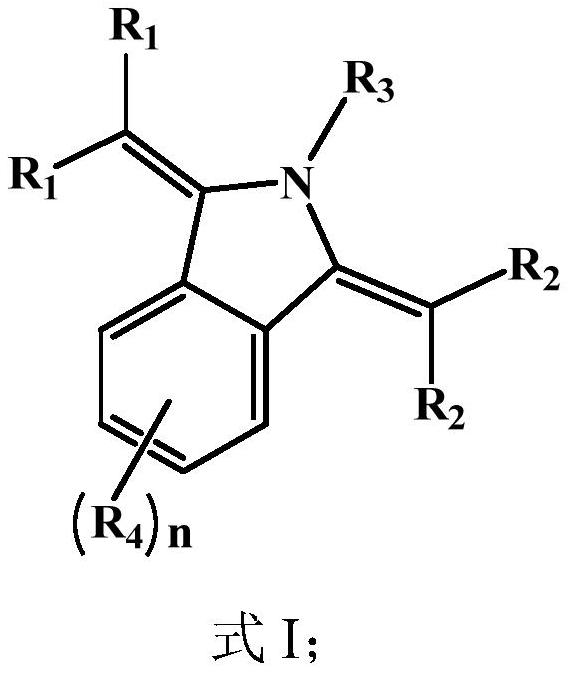
[0088] This embodiment provides an organic compound M1 with the following structure:
[0089]
[0090] The preparation method of this organic compound M1 comprises the steps:
[0091]
[0092] Add compound A (2.94g, 20mmol), compound B (2.46g, 20mmol), 150mL toluene, sodium tert-butoxide NaOt-Bu (2.88g, 30mmol) and tri(di Benzylideneacetone) Dipalladium Pd 2 (dba) 3 (0.18g, 0.2mmol), and then reacted at 120°C for 24h under nitrogen atmosphere. Cool to room temperature, pour the reaction solution into 200 mL of ice water, extract three times with dichloromethane, combine the organic phases, spin into silica gel, and perform column chromatography (the mobile phase is a mixed solution of dichloromethane and n-hexane with a volume ratio of 1:1) Separate and purify to obtain compound C.
[0093] Characterization results of compound C:
[0094] 1 H-NMR (400MHz, CDCl 3 ): δ8.74-8.69 (m, 2H), 7.90 (t, J = 4.5Hz, 2H), 7.83 (t, J = 4.4Hz, 2H), 7.55-7.50 (m, 2H);
[0095] ...
Embodiment 2
[0107] This embodiment provides an organic compound M2 with the following structure:
[0108]
[0109] The preparation method of this organic compound M2 comprises the steps:
[0110]
[0111] Add compound A (2.94g, 20mmol), compound B-2 (2.51g, 20mmol), 150mL toluene, sodium tert-butoxide NaOt-Bu (2.88g, 30mmol) and three (dibenzylideneacetone)dipalladium Pd 2 (dba)3 (0.18g, 0.2mmol), and then reacted at 120°C for 24h under nitrogen atmosphere. Cool to room temperature, pour the reaction solution into 200 mL of ice water, extract three times with dichloromethane, combine the organic phases, spin into silica gel, and perform column chromatography (the mobile phase is a mixed solution of dichloromethane and n-hexane with a volume ratio of 1:1) Separation and purification yielded compound C-2.
[0112] Characterization results of compound C-2:
[0113] 1 H-NMR (400MHz, CDCl 3 ): δ8.09(s, 2H), 7.92(t, J=4.4Hz, 2H), 7.82(t, J=4.5Hz, 2H);
[0114] 13 C-NMR (100MHz, CD...
Embodiment 3
[0121] This embodiment provides an organic compound M3 with the following structure:
[0122]
[0123] The preparation method of this organic compound M3 comprises the steps:
[0124]
[0125] Add compound A (2.94g, 20mmol), compound B-3 (2.44g, 20mmol), 150mL of toluene, sodium tert-butoxide NaOt-Bu (2.88g, 30mmol) and three (dibenzylideneacetone)dipalladium Pd 2 (dba) 3 (0.18g, 0.2mmol), and then reacted at 120°C for 24h under nitrogen atmosphere. Cool to room temperature, pour the reaction solution into 200 mL of ice water, extract three times with dichloromethane, combine the organic phases, spin into silica gel, and perform column chromatography (the mobile phase is a mixed solution of dichloromethane and n-hexane with a volume ratio of 1:1) Separation and purification yielded compound C-3.
[0126] Characterization results of compound C-3:
[0127] 1 H-NMR (400MHz, CDCl 3 ): δ7.91(dd, J=5.6,3.4Hz,2H),7.82(dd,J=5.6,3.4Hz,2H),7.55-7.48(m,2H),7.45-7.38(m,1H), ...
PUM
| Property | Measurement | Unit |
|---|---|---|
| glass transition temperature | aaaaa | aaaaa |
Abstract
Description
Claims
Application Information
 - R&D Engineer
- R&D Manager
- IP Professional
- Industry Leading Data Capabilities
- Powerful AI technology
- Patent DNA Extraction
Browse by: Latest US Patents, China's latest patents, Technical Efficacy Thesaurus, Application Domain, Technology Topic, Popular Technical Reports.
© 2024 PatSnap. All rights reserved.Legal|Privacy policy|Modern Slavery Act Transparency Statement|Sitemap|About US| Contact US: help@patsnap.com