Solar cell electrode printing method
A technology for solar cells and printing methods, applied in circuits, electrical components, photovoltaic power generation, etc., can solve problems such as screen plate damage, unevenness, increased probability of battery cracking, etc., to improve the pass rate, improve accuracy, The effect of reducing the probability of cracking
- Summary
- Abstract
- Description
- Claims
- Application Information
AI Technical Summary
Problems solved by technology
Method used
Image
Examples
Embodiment 1
[0082] This embodiment provides a method for printing the back electrode of a solar cell, including the following steps:
[0083] S1. Cleaning and making texture: at a temperature of 80-90°C, put the silicon base in 3% to 5% NaOH solution for 2 minutes, clean the surface of the silicon base to remove the surface damage of the silicon wafer, and continue to place it in the NaOH solution for 10 minutes , the surface is textured to make pyramid suede, so as to increase the specific surface area to receive more photons, while reducing the reflection of incident light. The temperature and the concentration of NaOH solution are conventional settings. For the convenience of implementation, the setting temperature is 90°C, the concentration of NaOH solution is 5% during cleaning, the setting temperature is 80°C, and the concentration of NaOH solution is 3% during cashmere making.
[0084] S2. Diffusion: Put the texturized silicon wafer into a diffusion furnace, and at a temperature of...
Embodiment 2
[0100] This embodiment provides a method for printing the back electrode of a solar cell, the steps are similar to those in Embodiment 1, the only difference being:
[0101] S7. Coating: In this embodiment, plate-type PECVD is used for coating, and a silicon nitride film is coated on the surface of the silicon wafer after the alkali polishing treatment, specifically including:
[0102] In the plate type PECVD, the silicon nitride film is coated on the surface of the silicon wafer after alkali polishing. blue. The front film process remains unchanged.
[0103] S8. Laser slotting: the positioning point power or frequency of the laser slotting equipment used in this embodiment cannot be adjusted separately. Set the position graph speed of the positioning point on the back to 1150mm / s, the power of the positioning point on the back is 5W, and the frequency is 12KHz , so that the back anchor points are white.
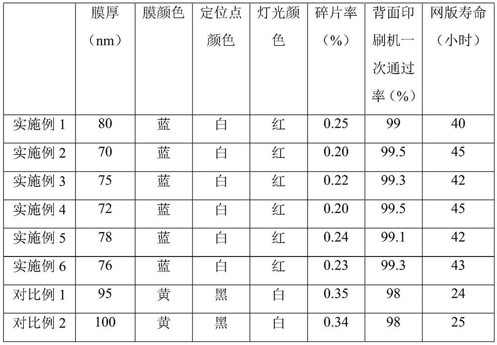
[0104] According to statistics on the production of solar cell sheet...
Embodiment 3
[0106] This embodiment provides a method for printing the back electrode of a solar cell, the steps are similar to those in Embodiment 1, the only difference being:
[0107] S7. Coating: In this embodiment, plate-type PECVD is used for coating, and a silicon nitride film is coated on the surface of the silicon wafer after the alkali polishing treatment, specifically including:
[0108] In the plate type PECVD, the silicon nitride film is coated on the surface of the silicon wafer after alkali polishing. blue. The front film process remains unchanged.
[0109] S8. Laser slotting: the power or frequency of the positioning point of the laser slotting equipment used in this embodiment cannot be adjusted separately. The position graph speed of the positioning point on the back is set to 1125mm / s, the power of the positioning point on the back is 4W, and the frequency is 15KHz. , so that the back anchor points are white.
[0110] Statistics were made on the production of solar ce...
PUM
| Property | Measurement | Unit |
|---|---|---|
| thickness | aaaaa | aaaaa |
| electrical resistance | aaaaa | aaaaa |
Abstract
Description
Claims
Application Information
 - Generate Ideas
- Intellectual Property
- Life Sciences
- Materials
- Tech Scout
- Unparalleled Data Quality
- Higher Quality Content
- 60% Fewer Hallucinations
Browse by: Latest US Patents, China's latest patents, Technical Efficacy Thesaurus, Application Domain, Technology Topic, Popular Technical Reports.
© 2025 PatSnap. All rights reserved.Legal|Privacy policy|Modern Slavery Act Transparency Statement|Sitemap|About US| Contact US: help@patsnap.com

