High-barrier SiC JBS device and preparation method thereof
A device and high-potential technology, which is applied in semiconductor/solid-state device manufacturing, semiconductor devices, electrical components, etc., can solve problems such as large chip reverse leakage
- Summary
- Abstract
- Description
- Claims
- Application Information
AI Technical Summary
Problems solved by technology
Method used
Image

Examples
Embodiment 1
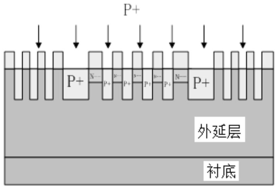
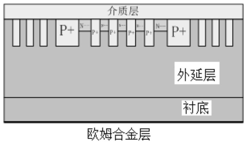
[0102] Such as Figure 1f As shown, the high barrier SiC JBS device provided in this embodiment includes a first electrode layer, a SiC substrate, an N-SiC epitaxial layer, a second electrode layer, a dielectric layer and a PI layer arranged from top to bottom.
[0103] Among them, the first electrode layer uses Ni as the SiC ohmic alloy layer, and the Ti / Ni / Ag back metal layer is thickened, with a thickness of 1.0um-1.2um; the thickness of the SiC substrate is 250um-350um; the N-SiC epitaxial layer The thickness is 6um-30um, which is doped with nitrogen ions and phosphorus ions, and the doping concentration is 1e15cm -3 -3e16cm -3 ; The second electrode layer is a Ti metal layer with a thickness of 150nm-200nm; the dielectric layer is SiO 2 The thickness of the layer is 0.8um-1.0um; the thickness of the PI layer is 10um-30um.
[0104] The N-SiC epitaxial layer includes a junction barrier region extending from the upper surface of the epitaxial layer into the epitaxial laye...
Embodiment 2
[0123] The structure of the high barrier SiC JBS device provided in this example is the same as that of Example 1, and its preparation method is as follows:
[0124] Step 1: providing a SiC substrate and an N-SiC epitaxial layer on the SiC substrate;
[0125] Step 2: forming a junction barrier region and a terminal region on the upper surface of the epitaxial layer:
[0126] (1) Cleaning the N-SiC wafer;
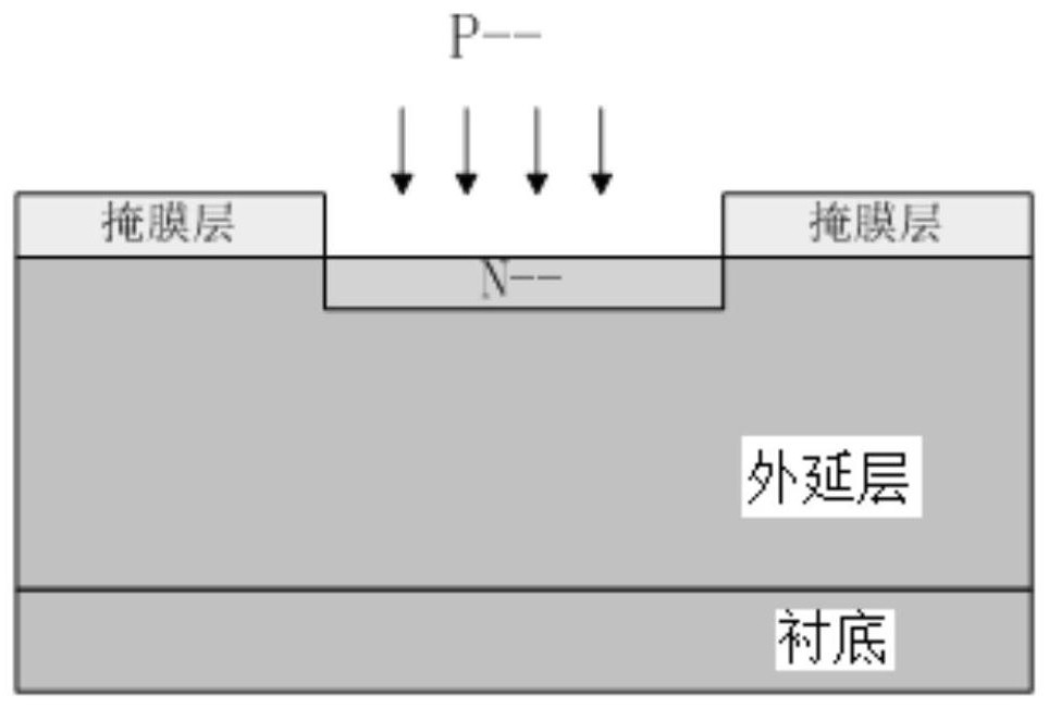
[0127] (2) An etching mask is grown on the surface of the SiC wafer, and a second mask is used to perform photolithography and etching to form a second implant mask, and a deep implantation of P-type impurities (P+ implantation) is performed on the etched area, The depth of injection is 1.0um, and the injection concentration is 1e19cm -3 -5e20cm -3 , forming a JBS structure;
[0128] (3) Remove the mask and clean the wafer;
[0129] (4) An etching mask is grown on the surface of the wafer in step (3), and the active region is photolithographically and etched using the f...
Embodiment 3
[0133] The structure of the high barrier SiC JBS device provided in this example is the same as that of Example 1, and its preparation method is as follows:
[0134] Step 1: providing a SiC substrate and an N-- / N-SiC epitaxial layer on the SiC substrate;
[0135] Step 2: forming a junction barrier region and a terminal region on the upper surface of the epitaxial layer:
[0136] (1) Clean the N-- / N-SiC wafer;
[0137] (2) Growing an etching mask on the surface of the SiC wafer, using the second mask plate, performing photolithography and etching to form a second implant mask, and performing deep implantation of P-type impurities (P+ implantation) into the etched area, The depth of injection is 1.0um, and the injection concentration is 1e19cm -3 -5e20cm -3 , forming a junction barrier region in the active region and forming a terminal region at the same time;
[0138] (3) Remove the mask, clean the wafer, and perform annealing treatment.
[0139] Step 3-6: Same as Example ...
PUM
| Property | Measurement | Unit |
|---|---|---|
| Thickness | aaaaa | aaaaa |
| Thickness | aaaaa | aaaaa |
| Thickness | aaaaa | aaaaa |
Abstract
Description
Claims
Application Information
 - R&D
- Intellectual Property
- Life Sciences
- Materials
- Tech Scout
- Unparalleled Data Quality
- Higher Quality Content
- 60% Fewer Hallucinations
Browse by: Latest US Patents, China's latest patents, Technical Efficacy Thesaurus, Application Domain, Technology Topic, Popular Technical Reports.
© 2025 PatSnap. All rights reserved.Legal|Privacy policy|Modern Slavery Act Transparency Statement|Sitemap|About US| Contact US: help@patsnap.com