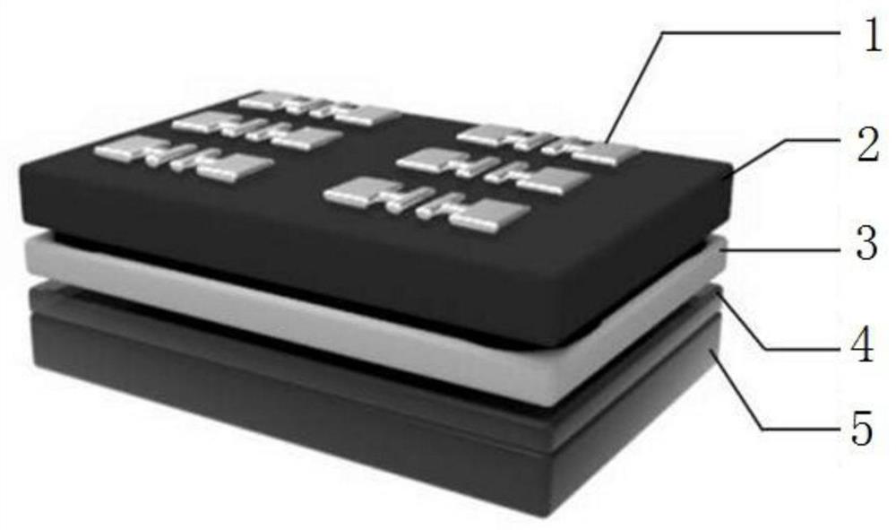
Self-assembled bipolar organic field effect transistor memory and preparation method thereof
A self-assembly, organic field technology, used in semiconductor/solid-state device manufacturing, semiconductor devices, electric solid-state devices, etc., can solve the problem of poor performance reproducibility of OFET devices, difficult OTS monolayer surface roughness reproducibility, and inability to guarantee OTS problems such as the surface quality of the single-layer film, to achieve the effect of reducing the difficulty of preparation, good storage performance, and easy operation
- Summary
- Abstract
- Description
- Claims
- Application Information
AI Technical Summary
Problems solved by technology
Method used
Image

Examples
Embodiment 1
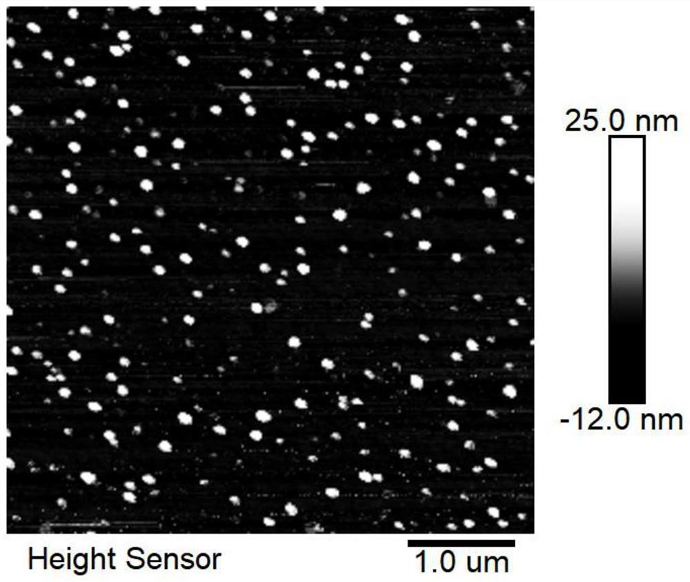
[0036] (1) Prepare polystyrene (PS) solution with a concentration of 3 mg / mL, which needs to be prepared at least 12 hours in advance to ensure that the polystyrene is fully dissolved; prepare octadecyltrichlorosilane (OTS solution) with a concentration of 3 mg / mL ; Low boiling point solvents are toluene without additional treatment;
[0037] (2) Select a heavily doped silicon wafer as the substrate, and sequentially form a gate electrode and a gate insulating layer on the substrate. The gate electrode is made of n-type doped silicon material, and the gate insulating layer is made of SiO 2 , with a thickness of 50nm, to make a substrate; place the substrate in a beaker, add acetone to immerse the silicon wafer substrate, ultrasonicate for 15 minutes, and pour off the acetone; then add ethanol and deionized water, and repeat the treatment of the silicon wafer substrate with acetone same operation. Then dry the surface with nitrogen and place it in an oven at 120°C for 30 minut...
Embodiment 2
[0044] (1) Prepare polystyrene (PS) solution with a concentration of 2mg / mL, which needs to be prepared at least 12 hours in advance to ensure that the polystyrene is fully dissolved; prepare octadecyltrichlorosilane (OTS solution) with a concentration of 2mg / mL ; Low boiling point solvents are toluene without additional treatment;
[0045] (2) Select a heavily doped silicon wafer as the substrate, and form a gate electrode and a gate insulating layer sequentially on the substrate. The gate electrode is made of aluminum, and the gate insulating layer is made of aluminum oxide with a thickness of 100 nm to make the substrate; Place the substrate in a beaker, add acetone to immerse the silicon wafer substrate, sonicate for 15 minutes, and pour off the acetone; then add ethanol and deionized water, and repeat the same operation as when treating the silicon wafer substrate with acetone. Then dry the surface with nitrogen and place it in an oven at 120°C for 30 minutes to dry the s...
Embodiment 3
[0052] (1) Configure polymethyl methacrylate (PMMA) solution with a concentration of 4 mg / mL, which needs to be prepared at least 12 hours in advance to ensure that polystyrene is fully dissolved; configure octadecyltrichlorosilane (OTS solution) with a concentration of 4mg / mL; low boiling point solvents are toluene without additional treatment;
[0053] (2) Select a heavily doped silicon wafer as the substrate, and form a gate electrode and a gate insulating layer sequentially on the substrate. The gate electrode is made of copper, and the gate insulating layer is made of polyvinylpyrrolidone with a thickness of 150nm to make the substrate; Place the substrate in a beaker, add acetone to immerse the silicon wafer substrate, sonicate for 15 minutes, and pour off the acetone; then add ethanol and deionized water, and repeat the same operation as when treating the silicon wafer substrate with acetone. Then dry the surface with nitrogen and place it in an oven at 120°C for 30 min...
PUM
| Property | Measurement | Unit |
|---|---|---|
| thickness | aaaaa | aaaaa |
| thickness | aaaaa | aaaaa |
| thickness | aaaaa | aaaaa |
Abstract
Description
Claims
Application Information
 - R&D
- Intellectual Property
- Life Sciences
- Materials
- Tech Scout
- Unparalleled Data Quality
- Higher Quality Content
- 60% Fewer Hallucinations
Browse by: Latest US Patents, China's latest patents, Technical Efficacy Thesaurus, Application Domain, Technology Topic, Popular Technical Reports.
© 2025 PatSnap. All rights reserved.Legal|Privacy policy|Modern Slavery Act Transparency Statement|Sitemap|About US| Contact US: help@patsnap.com