Trench type MPS diode cellular structure based on SiC substrate

A diode and trench technology, applied in the cell structure field of trench MPS diodes based on SiC substrates, can solve the problems of unstable device performance, uneven current distribution, and reduced Schottky barrier, and achieve elimination The effect of snapback effect, reduction of surface electric field strength, and enhancement of working stability

Active Publication Date: 2021-01-19
CHONGQING UNIV OF POSTS & TELECOMM
View PDF16 Cites 0 Cited by
  • Summary
  • Abstract
  • Description
  • Claims
  • Application Information

AI Technical Summary

Problems solved by technology

It has two disadvantages: first, when the forward bias voltage is applied, the Schottky contact is first turned on, and only one kind of carrier in the device participates in conduction, and the device works in a unipolar conduction state at this time; When the voltage gradually increases, the P+ ohmic contact area begins to conduct, and the device begins to convert from unipolar conduction mode to bipolar conduction mode. At this time, the holes in the device participate in conduction, but at the same time, the device will produce a voltage rebound phenomenon. , that is, the snapback effect, which will seriously affect the forward conduction performance of the device, resulting in unstable working performance of the device; the snapback effect will make the internal current distribution of the device uneven and the device current too large, and the excessive current will lead to uneven temperature distribution inside the device , where the current is too high, the temperature is too high, causing the device to be burned
Second, the P+ ohmic contact area of ​​the traditional SiC MPS diode is closely connected with the Schottky contact area. Under the external reverse bias voltage, as the voltage increases, the surface electric field of the Schottky contact area continues to increase. , which will lead to a continuous decrease in the Schottky barrier, resulting in a greater increase in the reverse leakage current of the device as the reverse bias voltage increases

Method used


Image

  • Trench type MPS diode cellular structure based on SiC substrate
  • Trench type MPS diode cellular structure based on SiC substrate
  • Trench type MPS diode cellular structure based on SiC substrate

Examples


Embodiment 1

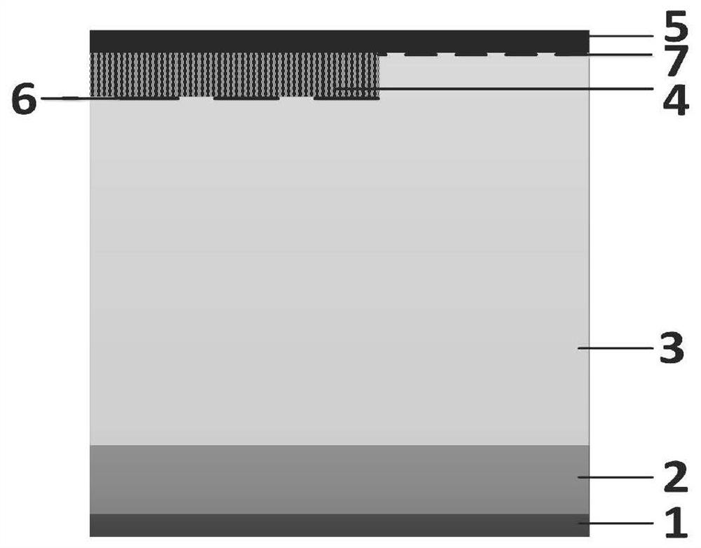
[0043] Such as figure 2 As shown, the present invention relates to a trench type MPS diode cell structure based on a SiC substrate, the device includes a cathode metal Al contact region 1, an N+ high-concentration substrate layer 2, an N- low-concentration epitaxial layer 3, and a P+ emitter region 4 , Trench HfO 2 Dielectric region 5 , anode metal Ni contact region 6 , P+N-junction contact surface 7 and anode metal NiN-Schottky junction contact surface 8 .

[0044] The cathode metal Al contact region 1 is located on the lower surface of the N+ high-concentration substrate layer 2 , and the cathode metal Al contact region 1 has a width of 5 μm and a thickness of 0.1 μm.

[0045] The N+ high-concentration substrate layer 2 is respectively located on the lower surface of the N- low-concentration epitaxial layer 3 and the upper surface of the cathode metal Al contact region 1; the N+ high-concentration substrate layer 2 is doped silicon carbide with a width of 5 μm and a thickn...

Embodiment 2

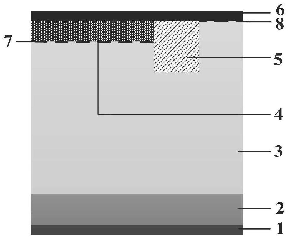
[0053] Such as image 3 As shown, the present invention relates to a trench type MPS diode cell structure based on a SiC substrate, the device includes a cathode metal Al contact region 1, an N+ high-concentration substrate layer 2, an N- low-concentration epitaxial layer 3, and a P+ emitter region 4 , P-type guard ring 5, trench SiO 2 Dielectric region 6 , anode metal Ni contact region 7 , P+N-junction contact surface 8 and anode metal NiN-Schottky junction contact surface 9 .

[0054] The cathode metal Al contact region 1 is located on the lower surface of the N+ high-concentration substrate layer 2 , and the cathode metal Al contact region 1 has a width of 5 μm and a thickness of 0.1 μm.

[0055] The N+ high-concentration substrate layer 2 is respectively located on the lower surface of the N- low-concentration epitaxial layer 3 and the upper surface of the cathode metal Al contact region 1; the N+ high-concentration substrate layer 2 is doped silicon carbide with a width ...

Embodiment 3

[0064] Such as Figure 4 As shown, the present invention relates to a trench type MPS diode cell structure based on a SiC substrate, the device includes a cathode metal Al contact region 1, an N+ high-concentration substrate layer 2, an N- low-concentration epitaxial layer 3, and a P+ emitter region 4 , P-type guard ring 5, SiO 2 Isolation ring 6 , heavily doped N+ polysilicon 7 , anode metal Ni contact region 8 , P+N-junction contact surface 9 and anode metal NiN-Schottky junction contact surface 10 .

[0065] The cathode metal Al contact region 1 is located on the lower surface of the N+ high-concentration substrate layer 2 , and the cathode metal Al contact region 1 has a width of 5 μm and a thickness of 0.1 μm.

[0066]The N+ high-concentration substrate layer 2 is respectively located on the lower surface of the N- low-concentration epitaxial layer 3 and the upper surface of the cathode metal Al contact region 1; the N+ high-concentration substrate layer 2 is doped silic...


PUM

PropertyMeasurementUnit
lengthaaaaaaaaaa
widthaaaaaaaaaa
widthaaaaaaaaaa

Abstract

The invention relates to a trench type MPS diode cellular structure based on a SiC substrate, and belongs to the technical field of semiconductors. On the basis of a conventional MPS device, a grooveSiO2 dielectric region and a P-type protection ring are introduced, and the structure has the advantages that (1) in a forward conduction unipolar conduction mode, the groove SiO2 dielectric region and the P-type protection ring have a blocking effect on electrons and prevent the electrons from directly flowing to a Schottky contact region, so the electrons are continuously accumulated below a P+emitter region; after the P + N junction reaches a turn-on voltage, holes are injected into the Nlow-concentration epitaxial layer, the device enters a bipolar conductive mode, so the voltage reboundphenomenon is effectively suppressed, and finally the snapback effect is eliminated; (2) during reverse breakdown, the groove SiO2 dielectric region and the P-type protection ring shield the surface electric field of the Schottky junction, and the maximum surface electric field is introduced into the body, so that the device is subjected to breakdown in the body, and the reverse leakage current ofthe device is reduced.

Description

technical field [0001] The invention belongs to the technical field of semiconductors and relates to a trench type MPS diode cell structure based on a SiC substrate. Background technique [0002] Silicon carbide (SiC) material, as a representative of the third-generation semiconductor material, has many advantages, such as a large band gap (about three times that of silicon), a large critical breakdown electric field (about the critical ten times the breakdown electric field), great thermal conductivity (about three times that of silicon), high saturation electron drift velocity (about twice the saturation electron drift velocity of silicon) and dielectric The constant is very low and so on. First of all, silicon carbide (SiC) semiconductor materials can be used to manufacture high-frequency high-power semiconductor devices with high temperature resistance, improve the stability of the devices, and be better used in manufacturing, smart grids, aerospace, wind and thermal po...

Claims


Application Information

Patent Timeline
Patent Type & Authority Applications(China)
IPC IPC(8): H01L29/861H01L29/868H01L29/06
CPCH01L29/8611H01L29/868H01L29/0603H01L29/0684
Inventor 陈伟中秦海峰王礼祥许峰黄义
Owner CHONGQING UNIV OF POSTS & TELECOMM
Why Eureka
Try Eureka