Overlay Error Measuring Device, Measuring Method and Optimizing Method

An overlay error and measurement device technology, applied in the lithography-related field, can solve the problems of increasingly demanding overlay mark size requirements, difficulty in speed and accuracy, difficulty in real overlay error, etc., and achieves the optimization of overlay error measurement device , excellent performance, the effect of avoiding motion errors

Active Publication Date: 2021-07-27
HUAZHONG UNIV OF SCI & TECH
View PDF9 Cites 0 Cited by
  • Summary
  • Abstract
  • Description
  • Claims
  • Application Information

AI Technical Summary

Problems solved by technology

[0020] Although this device does not need to limit the period of the overlay mark when measuring the overlay error (using the zero-order diffracted light of the overlay mark, that is, the mirror reflection light to obtain its Mueller matrix, the reflection angle is not affected by the period of the overlay mark. influence), but the traditional Mueller matrix ellipsometer often has moving parts that interfere with the measurement results, and the measurement is time-consuming (usually takes several seconds), so its practical application in the field of overlay error measurement faces the dilemma of speed and accuracy
[0021] In addition, with the continuation of Moore's Law, semiconductor devices continue to develop towards the trend of miniaturization, and the requirements for the size of overlay marks are becoming more and more stringent, which poses a challenge to the existing measurement devices
On the other hand, semiconductor devices are changing from a two-dimensional structure to a three-dimensional structure (for example, the three-dimensional flash memory structure has been stacked to more than a hundred layers). Due to factors such as stress, it is difficult for the real overlay error of the device area to pass through the scribed groove. Accurate characterization of overlay marks in

Method used


Image

  • Overlay Error Measuring Device, Measuring Method and Optimizing Method
  • Overlay Error Measuring Device, Measuring Method and Optimizing Method
  • Overlay Error Measuring Device, Measuring Method and Optimizing Method

Examples


Embodiment Construction

[0070] In order to make the object, technical solution and advantages of the present invention clearer, the present invention will be further described in detail below in conjunction with the accompanying drawings and embodiments. It should be understood that the specific embodiments described here are only used to explain the present invention, not to limit the present invention. In addition, the technical features involved in the various embodiments of the present invention described below can be combined with each other as long as they do not constitute a conflict with each other.

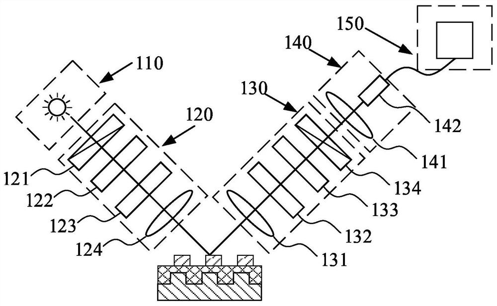
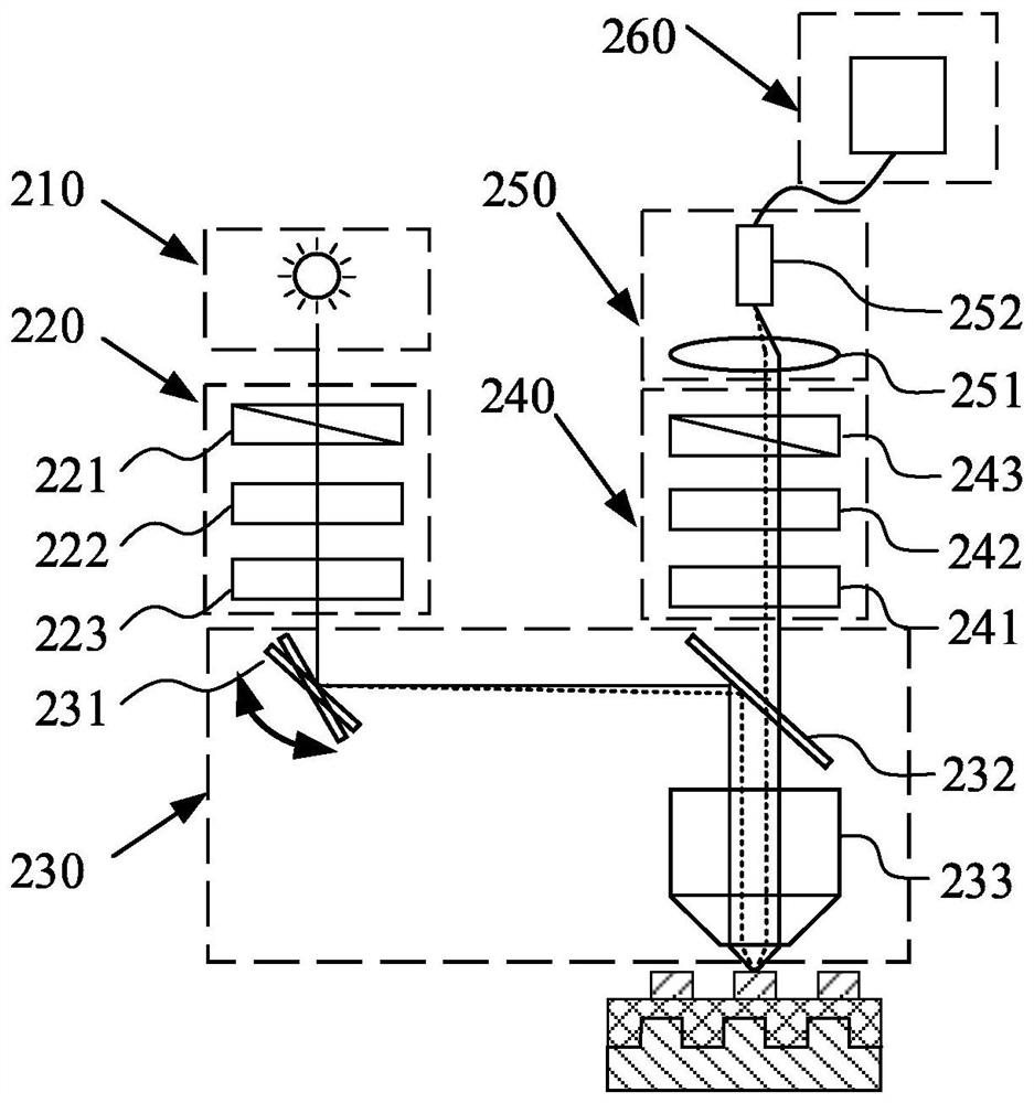
[0071] see figure 1 , the first form of the overlay error measurement device provided by the present invention, the device includes an illumination system 110, a polarizer arm 120, an analyzer arm 130, a detection system 140 and a data processing system 150, wherein:

[0072] The lighting system 110 is used for generating detection light. In the embodiment of the present disclosure, the illumi...


PUM


Abstract

The invention belongs to the technical field related to lithography, and discloses an overlay error measurement device and its measurement method and optimization method. The device includes: an illumination system; It includes a polarizer, a first phase retarder, a second phase retarder and a first lens group in sequence; an analyzer arm arranged symmetrically with the polarizer arm along the normal line of the surface of the overlay sample to be measured, and the analyzer arm is arranged along the optical path It includes the second lens group, the third phase retarder, the fourth phase retarder and the polarizer in turn; the detection system arranged on the optical path of the polarizer arm, the detection system converges the beam demodulated by the polarizer arm and sends the beam to A data processing system. The data processing system converts the light beam into a Mueller matrix, and obtains an overlay error according to the Mueller matrix. The overlay marking period of the overlay sample to be tested in the application is not limited, the measurement speed is fast, the measurement result is not disturbed by moving devices, the measurement accuracy is high, the robustness is good, and the application range is wide.

Description

technical field [0001] The invention belongs to the technical field related to photolithography, and more specifically relates to an overlay error measurement device, a measurement method and an optimization method thereof. Background technique [0002] Integrated Circuit (IC) is an indispensable part of modern production and life, photolithography is a key process in the manufacture of integrated circuits, and overlay error (Overlay) is an important parameter in the photolithography process. Overlay error refers to the alignment error between the current layer (the pattern retained on the photoresist after exposure and development) and the reference layer (the existing pattern on the wafer) during exposure, that is, the relative to the design position of the current layer. Offset. Overlay accuracy is one of the three major indicators of lithography machines, and its size has a direct impact on device performance. Excessive overlay errors will lead to short circuits or open...

Claims


Application Information

Patent Timeline
Patent Type & Authority Patents(China)
IPC IPC(8): G03F7/20G01N21/956G01B11/00
CPCG01B11/00G01N21/95607G01N2021/95615G03F7/70508G03F7/70625G03F7/70633
Inventor 刘世元王鹏陈修国张劲松石雅婷
Owner HUAZHONG UNIV OF SCI & TECH
Why Eureka
Try Eureka