
Method for forming non-crystal layer in substrate by using gas cluster ionic beams

A gas cluster, ion beam technology, applied in the direction of ion implantation plating, coating, metal material coating process, etc., can solve the problem of uneven pit interface and so on

Inactive Publication Date: 2021-01-05
JIANGSU JICHUANG ATOMIC CLUSTER RES INST CO LTD
View PDF4 Cites 1 Cited by
  • Summary
  • Abstract
  • Description
  • Claims
  • Application Information

AI Technical Summary

Problems solved by technology

[0007] However, the conventional GCIB process still has various defects
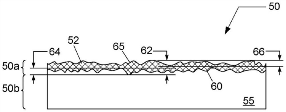
Even with the favorable results described above, the GCIB process produces a non-uniform dimpled interface between the GCIB-treated surface layer and the underlying untreated layer

Method used


Image

  • Method for forming non-crystal layer in substrate by using gas cluster ionic beams
  • Method for forming non-crystal layer in substrate by using gas cluster ionic beams
  • Method for forming non-crystal layer in substrate by using gas cluster ionic beams

Examples


Embodiment Construction

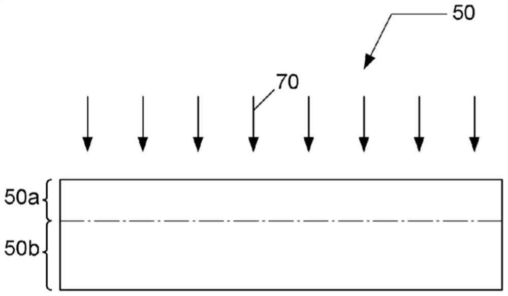
[0027]The operation steps are described in detail through several embodiments. In various embodiments, a method of using gas cluster ion beam (GCIB) processing to amorphize a layer including a silicon-containing film on a substrate is described. Those skilled in the relevant art will recognize that various embodiments may be implemented without one or more specific details, or with other alternative and / or additional methods, materials or components. In other cases, well-known structures, materials or operations are not shown or described in detail to avoid obscuring aspects of the various embodiments of the present invention. Similarly, for the purpose of explanation, specific numbers, materials and configurations are set forth in order to provide a thorough understanding of the present invention. However, the present invention can be implemented without specific details. In addition, it should be understood that the various embodiments shown in the figures are illustrative represe...


PUM


Abstract

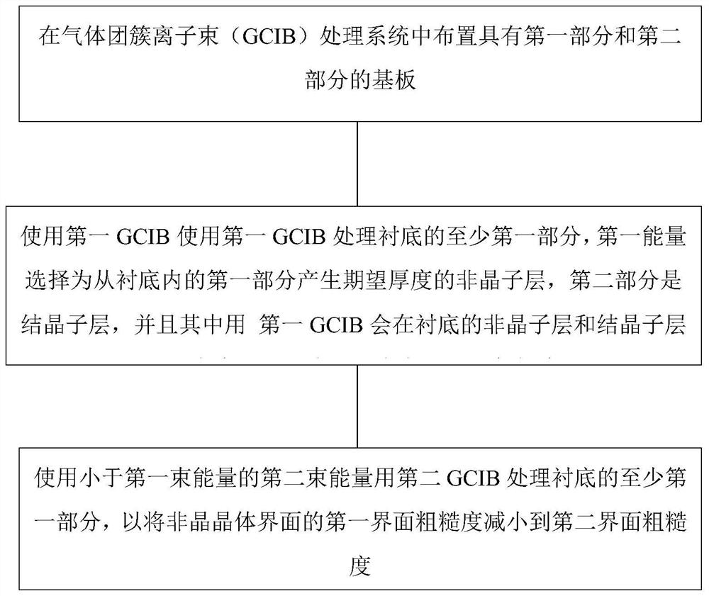
The invention discloses a method for forming a non-crystal layer in a substrate by using gas cluster ionic beams. The method is a method for non-crystallizing of a part of the substrate, and a part ofthe substrate provided with a first part and a second part in a gas cluster ionic beam treatment system is arranged; the substrate is treated by at least using a substrate treatment device; and the method for forming the non-crystal layer in the substrate by using the gas cluster ionic beams is provided, and the substrate is arranged in the gas cluster ionic beam treatment system. The method comprises the following steps: using a first beam of energy by a first GCIB (gas cluster ionic beam); generating a non-crystal sub-layer with required thickness on a first part area of the substrate through utilization of the first beam of energy, ensuring that a second part area of the substrate is a crystal sub-layer, and performing treatment on a non-crystal and crystal interface which generates anon-crystal-state first roughness interface and is positioned between the non-crystal layer and the crystal layer of the substrate by using the first GCIB; and then performing treatment on at least the first part area of the substrate by using the second GCIB and utilizing a second beam of energy being less than the first beam of energy, and ensuring that the first roughness interface is reduced to a second roughness interface.

Description

Technical field[0001]The invention relates to a method of forming an amorphous layer in a substrate. In particular, it is a method of forming an amorphous layer in a substrate by a gas cluster ion beam.Background technique[0002]The useful properties of semiconductor materials such as silicon, germanium, and gallium arsenide, as well as other semiconductors, depend on the purity and crystal structure of the semiconductor material. Generally, dopant atoms are incorporated into semiconductor materials to change electrical properties and form electronic PN junctions into the semiconductor surface through conventional ion implantation.[0003]In the conventional ion implantation process, ionized dopant atoms are physically deposited in the crystalline semiconductor material, but it is well known that when doing so, the crystal lattice of the semiconductor will be damaged by the implantation process. In order to make the implanted dopant atoms become electrically active in the semiconductor...

Claims


Application Information

Patent Timeline
IPC IPC(8): C23C14/48C23C14/16C23C14/54C23C14/58C23C14/04C23C14/02
CPCC23C14/48C23C14/16C23C14/54C23C14/5806C23C14/042C23C14/028
Inventor 曹路刘翊张同庆
Owner JIANGSU JICHUANG ATOMIC CLUSTER RES INST CO LTD
Learn More