Preparation method of ultrathin strip-shaped perovskite single crystal
A perovskite, ultra-thin technology, applied in the field of semiconductor optoelectronic materials preparation, can solve the problems of rare research on ultra-thin perovskite single crystals
- Summary
- Abstract
- Description
- Claims
- Application Information
AI Technical Summary
Problems solved by technology
Method used
Image
Examples
preparation example Construction
[0039] A method for preparing an ultra-thin strip-shaped perovskite single crystal, the steps of the method are described as follows:
[0040] 1) Combine AX and PbX 2 Dissolve in the precursor solvent according to the molar ratio of n:1, heat and stir to obtain three-dimensional (3D) perovskite APbX 3 The precursor solution, the concentration range is 0.001-0.02mol L -1 ;
[0041] 2) Add the above APbX 3 Take an appropriate amount of the precursor solution and drop it on the substrate, and place it in a glass vessel filled with anti-solvent, seal the glass vessel with a sealing film, and pierce a certain number of pinholes on the sealing film, and the needle The range of holes is 20-60, which is used to control the volatilization speed of solvent;
[0042] 3) Place the above-mentioned glass device quietly in an oven that has been heated up, and let it grow;
[0043] The structure of the ultrathin perovskite single crystal APbX described in 3 Among them, A is a short-chai...
Embodiment 1
[0059] In this embodiment, a method for preparing a high-quality, low-laser-threshold one-dimensional ultrathin ribbon-shaped perovskite single crystal includes the following steps:
[0060] 1) Combine MABr and PbBr 2 Dissolve in DMSO according to the molar ratio of 1:1, heat and stir to obtain 3D perovskite MAPbBr 3 The precursor solution, its concentration is 0.005mol L -1 ;
[0061] 2) the above MAPbBr 3 Take 30 μL of the precursor solution and drop it on the silica substrate, place it in a glass vessel filled with toluene, seal the glass vessel with a sealing film, and make 40 small holes;
[0062] 3) Slowly place the above-mentioned glass device in an oven at 40°C, and let it grow for 20 hours;
[0063] Among them, the ultrathin perovskite MAPbBr 3 The thickness of the single crystal is 100nm, and the emission wavelength is 515nm. At room temperature, laser lasing by pulsed optical pumping can be realized, and there is no continuous optical pumping lasing phenomenon....
Embodiment 2
[0065] In this embodiment, a method for preparing a high-quality, low-laser-threshold one-dimensional ultrathin ribbon-shaped perovskite single crystal includes the following steps:
[0066] 1) Combine CsBr and PbBr 2 Dissolve in DMF according to the molar ratio of 1.2:1, heat and stir to obtain 3D perovskite CsPbBr 3 The precursor solution, its concentration is 0.008mol L -1 ;
[0067] 2) the above CsPbBr 3 Take 20 μL of the precursor solution and drop it on the silica substrate, and place it in a glass vessel filled with toluene and dichloromethane, seal the glass vessel with a sealing film, and make 30 small holes;
[0068] 3) Slowly place the above-mentioned glass device in an oven at 30°C, and let it grow for 24 hours;
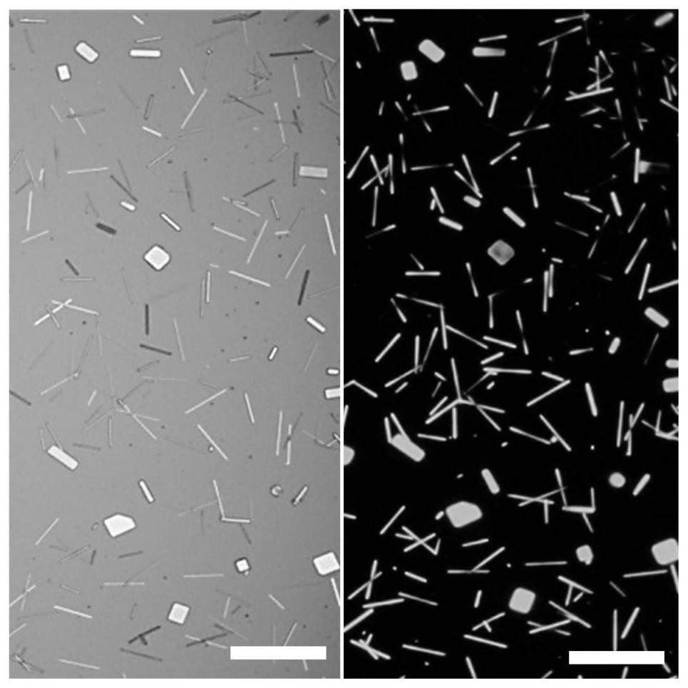
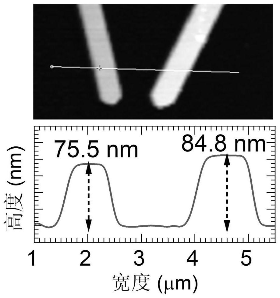
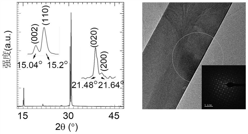
[0069] Among them, such as figure 1 Shown as CsPbBr 3 Brightfield (left panel) and darkfield (right panel) microscope images of a perovskite single crystal. Its appearance is ultra-thin ribbon, the thickness of the single crystal is 70nm, the aspec...
PUM
| Property | Measurement | Unit |
|---|---|---|
| Thickness | aaaaa | aaaaa |
| Luminous wavelength | aaaaa | aaaaa |
| Thickness | aaaaa | aaaaa |
Abstract
Description
Claims
Application Information
 - R&D
- Intellectual Property
- Life Sciences
- Materials
- Tech Scout
- Unparalleled Data Quality
- Higher Quality Content
- 60% Fewer Hallucinations
Browse by: Latest US Patents, China's latest patents, Technical Efficacy Thesaurus, Application Domain, Technology Topic, Popular Technical Reports.
© 2025 PatSnap. All rights reserved.Legal|Privacy policy|Modern Slavery Act Transparency Statement|Sitemap|About US| Contact US: help@patsnap.com


