Nanocrystalline amorphous composite coating, preparation method thereof and cutter
A composite coating and nanocrystalline technology, applied in coatings, metal material coating processes, vacuum evaporation plating and other directions, can solve problems such as short boards, improve wear resistance, reduce friction coefficient, and improve high temperature stability Effect
- Summary
- Abstract
- Description
- Claims
- Application Information
AI Technical Summary
Problems solved by technology
Method used
Image
Examples
Embodiment 1
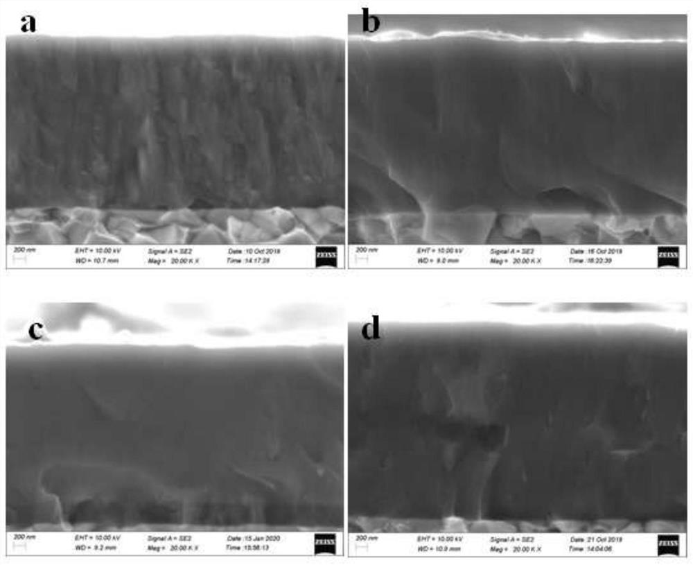
[0032] Deposition on the tool substrate by cathodic arc ion plating (Ti 0.3 al 0.6 (NbSiC)0.1 N) (Nb:Si:C atomic ratio is 3:5:2, the atomic composition is the theoretical design value) nanocrystalline amorphous single-layer composite coating: pass through the working gas N 2 And keep the pressure at 3.5Pa, the initial bias voltage is set to 30V, the rotation speed of the workpiece holder is about 1.58r / min, and 6 Tis are turned on at the same time 0.3 al 0.6 (NbSiC) 0.1 target, the arc source current is 200A, and the deposition time is 35min; the initial bias voltage is increased by 20V, and other process parameters remain unchanged, and the deposition time is 40min; the bias voltage continues to increase by 20V, and the deposition is continued for 40min to form a single layer of nanocrystalline amorphous Ti 0.3 al 0.6 (NbSiC) 0.1 N coating, figure 1 b is the fracture morphology of the coating.
Embodiment 2
[0034] Using cathodic arc ion plating technology to deposit Ti0.33Al0.67N / Ti0.3Al0.6(NbSiC)0.1N (the composition is the theoretical design value) nanocrystalline amorphous multilayer composite coating on the tool substrate: pass through the working gas N2 and Keep the pressure at 3.5Pa, set the initial bias voltage to 30V, and the rotation speed of the workpiece holder is about 1.58r / min. Only two TiAl targets are turned on, the arc source current is 200A, and the deposition time is 55min; the TiAl target is turned off, and four TiAl targets are turned on. 0.3 al 0.6 (NbSiC) 0.1 target, the arc source current is 200A, the initial bias voltage is increased by 20V, and the deposition time is 60min; the bias voltage continues to increase by 10V, and the deposition time is 70min, forming a nanocrystalline amorphous coating with a TiAlN / TiAlNbSiCN double-layer structure. figure 1 c is the fracture topography of the coating.
Embodiment 3
[0036] Deposition of Ti on Tool Substrate by Cathodic Arc Ion Plating Technology 0.3 al 0.53 (NbSiC) 0.13 N (B:C atomic ratio is 3:1, the atomic composition is the theoretical design value) nanocrystalline amorphous single-layer composite coating: the working gas N 2 And keep the pressure at 3.5Pa, set the bias voltage at 30V, the rotation speed of the workpiece holder is about 2.63r / min, and open 2 Ti at the same time 0.33 al 0.67 Target and 4 pieces of Ti 0.3 al 0.5 (NbSiC) 0.2 target, the arc source current is 200A, and the deposition time is 25min; the initial bias voltage is increased by 20V, and other process parameters remain unchanged, and the deposition time is 32min; the bias voltage continues to increase by 20V, and the deposition is continued for 32min to form a single layer of nanocrystalline amorphous Ti 0.3 al 0.53 (NbSiC) 0.13 N coating, figure 1 d is the fracture morphology of the coating.
[0037] 4. Turn off all arc sources, turn off the bias power...
PUM
| Property | Measurement | Unit |
|---|---|---|
| thickness | aaaaa | aaaaa |
| anti-oxidation temperature | aaaaa | aaaaa |
| thickness | aaaaa | aaaaa |
Abstract
Description
Claims
Application Information
 - R&D
- Intellectual Property
- Life Sciences
- Materials
- Tech Scout
- Unparalleled Data Quality
- Higher Quality Content
- 60% Fewer Hallucinations
Browse by: Latest US Patents, China's latest patents, Technical Efficacy Thesaurus, Application Domain, Technology Topic, Popular Technical Reports.
© 2025 PatSnap. All rights reserved.Legal|Privacy policy|Modern Slavery Act Transparency Statement|Sitemap|About US| Contact US: help@patsnap.com


