Method for preparing first scribed line and third scribed line of thin-film solar cell
A technology for solar cells and scribe lines, applied in circuits, photovoltaic power generation, electrical components, etc., can solve problems such as low light transmittance of insulating layers, affecting the effective area of thin-film solar cell components, and reducing parallel resistance
- Summary
- Abstract
- Description
- Claims
- Application Information
AI Technical Summary
Problems solved by technology
Method used
Image
Examples
Embodiment 1
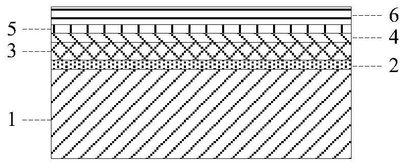
[0092] Soda-lime glass is used as the substrate 1 of the thin-film solar cell, and it is cleaned by the existing technology, and then a back electrode 2 of 800 nm is prepared on the substrate 1 by magnetron sputtering, and the back electrode 2 is made of metal molybdenum Composition, the absorption layer 3 is copper indium gallium selenide.
[0093] The following method is used to prepare and scribe thin film solar cells, including the following steps:
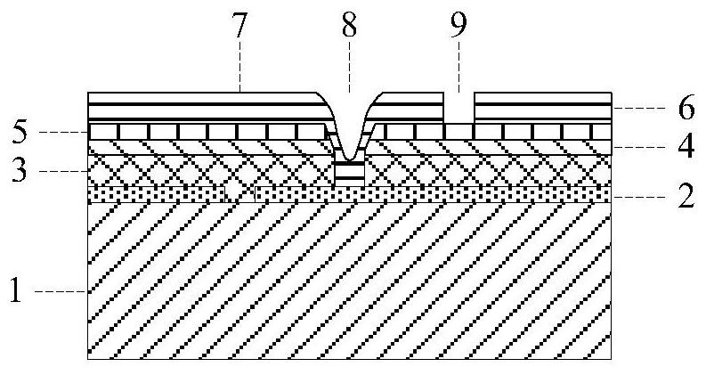
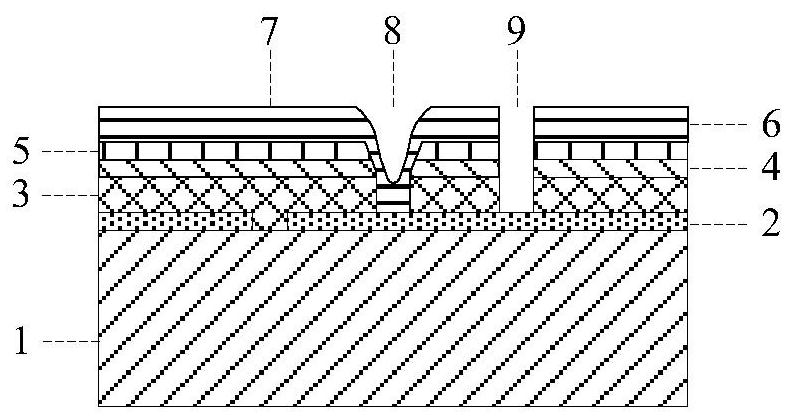
[0094] Step 1) Use a picosecond laser to generate a laser with a wavelength of 1064 nanometers and a frequency of 70 kHz at a power of 0.9 W. Under the condition of a marking speed of 2000 mm / s, the incident mode from the back (that is, incident from the glass surface) is adopted. Scribing the back electrode 2 to form a first scoring line 7;
[0095] Step 2) Adopt the method of screen printing to cover the insulating layer 11 on the first line 7, the insulating layer 11 is parallel to the first line 7, the composition of the ...
Embodiment 2
[0103] Soda-lime glass is used as the substrate 1 of the thin-film solar cell, and it is cleaned by the existing technology, and then a back electrode 2 of 800 nm is prepared on the substrate 1 by magnetron sputtering, and the back electrode 2 is made of metal molybdenum Composition, the absorption layer 3 is perovskite.
[0104] The following method is used to prepare and scribe thin film solar cells, including the following steps:
[0105] Step 1), step 3) to step 5) are identical with embodiment 1;
[0106] Step 2) Adopt high-power laser focused irradiation, the focused spot diameter is 15 microns, the power of the laser is 3W, and the laser with a wavelength of 532nm and a frequency of 400kHz is applied to the glass on the bottom surface of the first line 7. The melted glass is solidified on both sides of the first reticle 7 to form an insulating layer 11 with a thickness of 200 nanometers. The width of the insulating layer 11 is 4 microns wider than the first reticle 7, ...
Embodiment 3
[0111] Soda-lime glass is used as the substrate 1 of the thin-film solar cell, and it is cleaned by the existing technology, and then the back electrode 2 of 800 nanometers is prepared on the substrate 1 by magnetron sputtering, and the back electrode 2 is made of metal molybdenum, the absorption layer 3 is cadmium telluride.
[0112] The following method is used to prepare and scribe thin film solar cells, including the following steps:
[0113] Step 1), step 3) to step 5) are identical with embodiment 1;
[0114] Step 2) Inkjet printing is adopted, and an inkjet device is set at the same position as the laser head forming the first reticle 7, and the ink is replaced with silicon tetrachloride liquid, so that a layer is covered on the first reticle 7 The silicon tetrachloride liquid is then put into an oven at 260° C. for curing, and the holding time is 30 minutes. The silicon tetrachloride is converted into silicon dioxide, thus forming a transparent insulating layer 11, wh...
PUM
| Property | Measurement | Unit |
|---|---|---|
| Thickness | aaaaa | aaaaa |
| Power | aaaaa | aaaaa |
| Power | aaaaa | aaaaa |
Abstract
Description
Claims
Application Information
 - R&D
- Intellectual Property
- Life Sciences
- Materials
- Tech Scout
- Unparalleled Data Quality
- Higher Quality Content
- 60% Fewer Hallucinations
Browse by: Latest US Patents, China's latest patents, Technical Efficacy Thesaurus, Application Domain, Technology Topic, Popular Technical Reports.
© 2025 PatSnap. All rights reserved.Legal|Privacy policy|Modern Slavery Act Transparency Statement|Sitemap|About US| Contact US: help@patsnap.com


