
Method for manufacturing high-voltage VDMOS by adopting silicon-silicon bonding process

A silicon-silicon bond and bonding technology, which is applied in semiconductor/solid-state device manufacturing, electrical components, circuits, etc., can solve the problems of long preparation process time, low production efficiency, and wide transition zone, so as to reduce production costs and improve production Efficiency, effect of narrow transition zone

Pending Publication Date: 2020-11-06
杭州华芯微科技有限公司
View PDF0 Cites 1 Cited by
  • Summary
  • Abstract
  • Description
  • Claims
  • Application Information

AI Technical Summary

Problems solved by technology

However, for high-resistance epitaxy, when the epitaxy thickness reaches 100um, the preparation process takes a long time, and the single furnace process time exceeds 2.5 hours, the production efficiency is low, the preparation cost is high, and it will lead to many defects, poor resistivity consistency, and serious self-doping. Problems such as wide transition zone
Thus affecting product performance and increasing costs

Method used

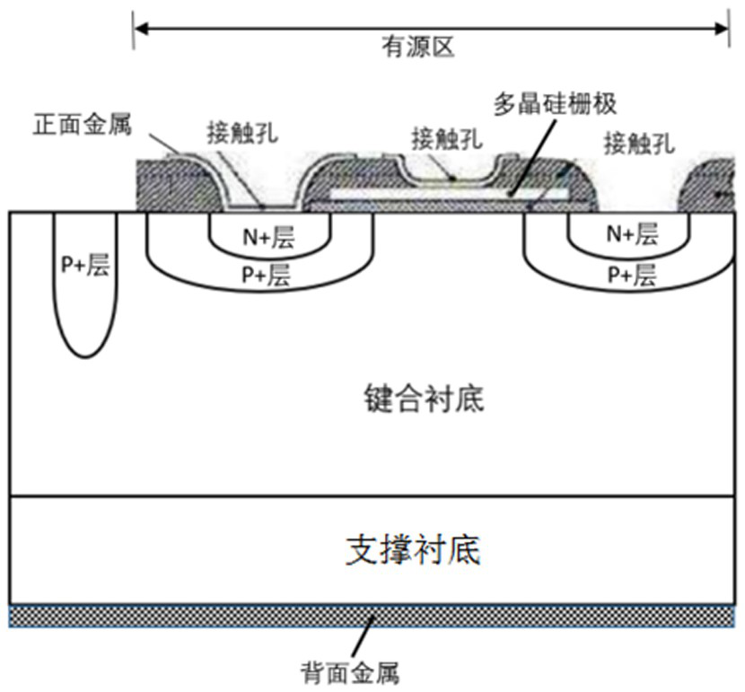
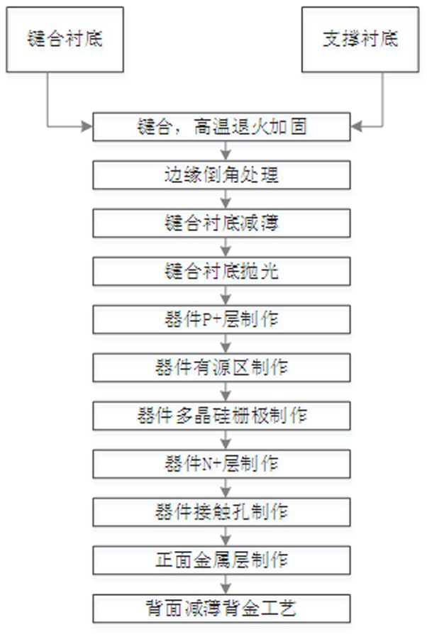

Image

  • Method for manufacturing high-voltage VDMOS by adopting silicon-silicon bonding process
  • Method for manufacturing high-voltage VDMOS by adopting silicon-silicon bonding process
  • Method for manufacturing high-voltage VDMOS by adopting silicon-silicon bonding process

Examples


Embodiment Construction

[0021] Hereinafter, exemplary embodiments of the present application will be described in detail with reference to the accompanying drawings. Apparently, the described embodiments are only some of the embodiments of the present application, rather than all the embodiments of the present application. It should be understood that the present application is not limited by the exemplary embodiments described here.

[0022] Application overview

[0023] The process flow of conventional high-voltage VDMOS products is as follows: Prepare the substrate—grow epitaxy on the substrate. The thickness of the epitaxy is usually 50~250um according to the voltage requirement. For high-voltage and high-voltage VDMOS products, the thickness and resistivity of the epitaxy are directly related to the withstand voltage. This also leads to long preparation process time when the epitaxial thickness reaches 100um, and the single furnace process time exceeds 2.5 hours, the production efficiency is low...


PUM

PropertyMeasurementUnit
Thicknessaaaaaaaaaa
Thicknessaaaaaaaaaa
Thicknessaaaaaaaaaa

Abstract

The invention relates to a method for manufacturing a high-voltage VDMOS by adopting a silicon-silicon bonding process. The method comprises the following steps: preparing a support substrate and a bonding substrate; carrying out silicon-silicon bonding on the support substrate and the bonding substrate, and carrying out high-temperature annealing and curing; carrying out a corrosion treatment onthe edge chamfers of the bonded support substrate and the bonding substrate; thinning the bonding substrate to a required thickness; and polishing the bonding substrate. The embodiment of the invention discloses a method for manufacturing a high-voltage VDMOS by adopting a silicon-silicon bonding process. The silicon-silicon bonding process is used; a silicon-silicon bonding sheet is prepared by bonding conventional CZ silicon substrate materials with different resistivity to replace an existing thick-film epitaxial wafer, a high-quality silicon substrate sheet meeting customer requirements isobtained, the production efficiency is improved, the production cost is reduced, a transition region of the obtained high-voltage VDMOS device is obviously narrowed, and the consistency of product parameters is better.

Description

technical field [0001] The invention relates to the technical field of semiconductor chip manufacturing technology, in particular to a method for manufacturing a high-voltage VDMOS using a silicon-silicon bonding technology. Background technique [0002] Conventional semiconductor manufacturing uses a variety of processes to form semiconductor devices in substrates. The substrate may be a small, thin, circular sliced ​​wafer of semiconducting material such as silicon. The semiconductor devices formed on the substrate may be discrete devices or integrated circuits. For example, a semiconductor device may consist of a single discrete power transistor, or may consist of many transistors or other electronic components such as resistors, capacitors, etc. electrically coupled together to form an integrated circuit. After the semiconductor devices are formed, the wafer is tested and diced to separate the individual dies in the wafer. [0003] High-voltage VDMOS is gradually deve...

Claims


Application Information

Patent Timeline
IPC IPC(8): H01L29/06H01L21/336H01L29/78
CPCH01L29/0684H01L29/66712H01L29/7802
Inventor 张峰冯羽
Owner 杭州华芯微科技有限公司
Learn More