Thinning method of lithium niobate wafer

A lithium niobate wafer technology, applied in the thinning field of lithium niobate wafers, can solve the problems of easy brittle failure, low hardness of lithium niobate processing thickness, deep subsurface damage layer, etc., to improve reliability , reduce the risk of fragmentation, and improve the quality of the effect

Active Publication Date: 2020-11-06
NINGBO CHIPEX SEMICON
View PDF3 Cites 6 Cited by
  • Summary
  • Abstract
  • Description
  • Claims
  • Application Information

AI Technical Summary

Problems solved by technology

[0005] The object of the present invention is to provide a method for thinning lithium niobate wafers, which is used to solve the grinding problem caused by lithium niobate low hardness, high brittleness, thin incoming material and processing thickness, and strong anisotropy. And the technical problems of brittle failure, deep subsurface damage layer and large cracking on the front and back of cutting are prone to occur during the cutting process

Method used


Image

  • Thinning method of lithium niobate wafer
  • Thinning method of lithium niobate wafer
  • Thinning method of lithium niobate wafer

Examples


Embodiment

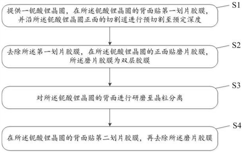
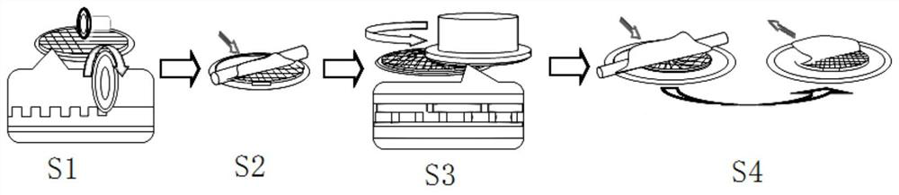
[0036] DBG (Dicing Before Grinding) is a commonly used process for wafer backside thinning and cutting. The cutting before grinding process is to reverse the original process of Dicing After Grinding (Dicing After Grinding). That is, the wafer is first half-cut, and then the wafer is divided into chips by back grinding. By using this technology, it is possible to minimize backside cracking and wafer breakage when the chips are divided, so that chips can be smoothly diced from large-sized wafers. Since the chipping phenomenon of the backside of the wafer is greatly reduced, it is possible to perform ultra-thin processing on the wafer while maintaining high flexural strength, so that a high-strength chip can be produced. In addition, since the chips are separated by the grinding process of the grinder, the risk of breakage of thin wafers during transportation can be effectively avoided. The pre-grinding dicing process can minimize the backside cracking caused by the dicing proc...


PUM


Abstract

The invention discloses a thinning method of a lithium niobate wafer, and belongs to the technical field of chip packaging. The thinning method of the lithium niobate wafer comprises the following steps: providing the lithium niobate wafer, pasting a first scribing adhesive film on the back surface of the lithium niobate wafer, and pre-cutting to a predetermined depth along a cutting channel on the front surface of the lithium niobate wafer; removing the first scribing adhesive film, and pasting an abrasive disc adhesive film on the front surface of the lithium niobate wafer, the abrasive discadhesive film being a double-layer adhesive film; grinding the back surface of the lithium niobate wafer until crystal grains are separated; and pasting a second scribing adhesive film on the back surface of the lithium niobate wafer, and then removing the grinding adhesive film. According to the invention, the pre-grinding cutting process of the lithium niobate wafer is realized. The phenomena of brittle failure, deep sub-surface damage layer, large cracks on the front and back surfaces of the chip and the like in the abrasive cutting process of the lithium niobate wafer in the prior art areavoided, the cracks on the front and back surfaces of the chip can be controlled within 10 microns, and the quality of a lithium niobate chip packaging product is ensured.

Description

technical field [0001] The invention relates to the technical field of chip packaging, in particular to a method for thinning a lithium niobate wafer. Background technique [0002] With the increasing demand for miniaturization, light weight and multi-functionality of electronic components, integrated circuits have higher and higher requirements for ultra-thin chips, MEMS, image sensors, stacked chips, multi-chip packaging, etc. Apply ultra-thin chips with a thickness of less than 50 μm. With the continuous development of integrated circuit chips in the direction of high density and thinness, in order to meet the above requirements of the chip, the backside of the wafer needs to be thinned and cut when the chip is packaged. [0003] Lithium niobate (LiNbO 3 ) crystals are widely used in optical storage, optical waveguides, and optical communication technologies due to their excellent piezoelectric, electro-optical and nonlinear optical properties, and are ideal substrate m...

Claims


Application Information

Patent Timeline
Patent Type & Authority Applications(China)
IPC IPC(8): H01L21/02H01L21/683H01L21/78B24B27/06B24B37/04B24B37/10B24B55/00
CPCH01L21/02013H01L21/02016H01L21/78H01L21/6836B24B27/0675B24B37/042B24B37/10B24B55/00H01L2221/68327H01L2221/68386
Inventor 何肇阳赵亚东罗立辉钟志明汪洋陈楚杰
Owner NINGBO CHIPEX SEMICON
Why Eureka
Try Eureka