A wafer debonding method

A debonding and wafer technology, applied in the field of microelectronic device packaging, can solve the problem that the thin wafer and the carrier can not be separated smoothly during the debonding process, achieve broad application prospects and market potential, avoid fragmentation risks, important strategic significance and social benefits Effect

Active Publication Date: 2022-02-11
珠海天成先进半导体科技有限公司
View PDF4 Cites 0 Cited by
  • Summary
  • Abstract
  • Description
  • Claims
  • Application Information

AI Technical Summary

Problems solved by technology

[0004] The purpose of the present invention is to solve the problem that the thin wafer and the carrier cannot be separated smoothly during the debonding process in the above-mentioned prior art, and to provide a wafer debonding method, which enables the temporary bonding glue to be detached smoothly through the pretreatment process, and avoids the risk of fragmentation

Method used


Image

  • A wafer debonding method
  • A wafer debonding method
  • A wafer debonding method

Examples


Embodiment 1

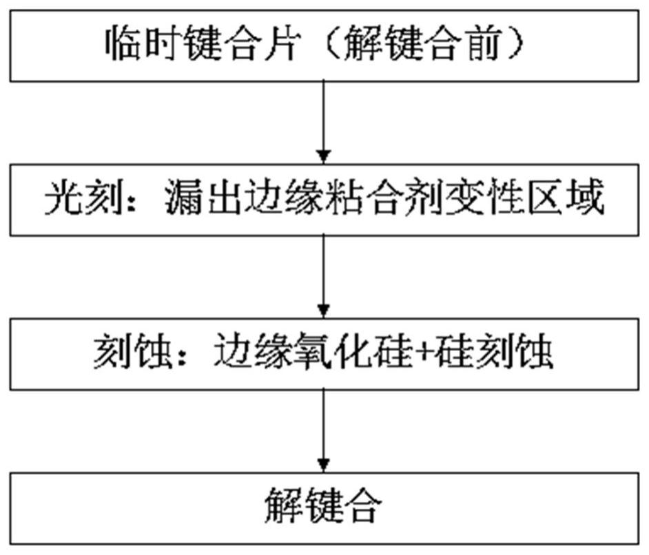
[0038] A wafer debonding method comprises the following steps:

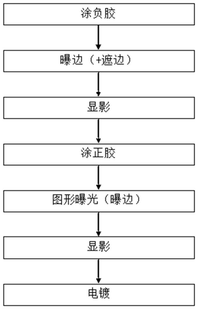
[0039] 1. The RDL layer is patterned before electroplating, and a cofferdam is prepared on the edge of the wafer through a photolithography process (coating, edge exposure, development). The photoresist is a negative photoresist, the model is JSR111, and the thickness of the glue is based on The process can be selected from 5 to 15 μm, and the width of the exposure edge can be selected from 0 to 5 mm (A1) according to the process. When the edge is exposed, the edge is covered with 1.4 mm to ensure that the edge is not covered with glue during electroplating and can conduct electricity normally, and the preparation of the cofferdam is completed. Afterwards, carry out normal patterning processing, and prepare the required pattern by applying glue, exposing and developing. The selected photoresist is a positive photoresist, the model is AZ4620, and the thickness can be selected from 5 to 20 μm according to the proces...

Embodiment 2

[0048] A wafer debonding method comprises the following steps:

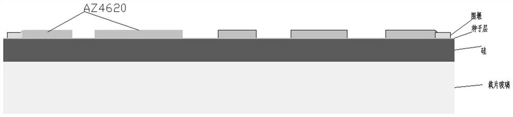
[0049] 1. Photolithography in the adhesive denatured area, glue coating, edge washing to expose the edge adhesive denaturation area, the photoresist model used in the photolithography process is AZ4620, the thickness of the photoresist is 20 μm, and the edge washing width is 6mm, such as Figure 9 shown;

[0050] 2. Use a dry degumming machine for PI etching. The PI material is JSR5100 with a thickness of 3-10 μm. The etching gas used to etch PI in the dry degumming machine is O 2 and CF 4 , O 2 and CF 4 The volume ratios are 75% to 95% and 5% to 25%, respectively, the microwave power is 1300W, the radio frequency power is 280W, the temperature is 20°C, and the etching time is 100s to 500s; the PI material in this example is JSR5100, The thickness is 4 μm, and the etching gas used for etching PI is O 2 and CF 4 , O 2 and CF 4 The flow rates are 800sccm and 40sccm respectively, the wave power is 1300W, the...


PUM

PropertyMeasurementUnit
thicknessaaaaaaaaaa
thicknessaaaaaaaaaa
thicknessaaaaaaaaaa

Abstract

A method for unbonding thin wafers, comprising the following steps: Step 1, etching and removing the silicon where the outer ring of the silicon wafer undergoes glue denaturation or glue overflow; and Step 2, unbonding the silicon wafer and the carrier. The etching removal method described in step 1 includes preparing a mask layer on the side of the wafer. The material of the mask layer is positive or negative photoresist, and the photoresist at the edge of the silicon wafer is removed through the exposure and development process. ; and then directly etch the outer ring of the silicon wafer through a dry etching process. Aiming at the problems of temporary bonding glue degeneration and "glue extrusion" of thin wafers, the present invention adopts a pre-treatment method for de-bonding, through pre-treatment processes such as mask preparation, etching and edge removal, etc. The silicon etching and removal of the glue overflow, and then the debonding process, solves the problem that the debonding cannot be carried out smoothly due to the denaturation of the temporary bonding glue, and avoids the risk of debris.

Description

technical field [0001] The invention belongs to the field of packaging of microelectronic devices, and in particular relates to a wafer unbonding method. Background technique [0002] Thin wafers are fragile and flexible, so it is usually necessary to use temporary bonding materials to bond them to the carrier. After a series of manufacturing processes, the wafers are then bonded by inputting light, heat, electricity, force or by soaking in a solution. detach from the support (referred to as "debonding"). However, when the bonded wafer undergoes subsequent processes, it usually involves acid, alkali, vacuum, and high and low temperature environments, which often cause the temporary bonding adhesive in some peripheral areas of the wafer to denature; or, during the bonding process In the process, due to heating and extrusion, the temporary bonding adhesive material will be extruded to the sides of the carrier and wafer to form adhesive residue. [0003] Whether the temporary...

Claims


Application Information

Patent Timeline
Patent Type & Authority Patents(China)
IPC IPC(8): H01L21/683
CPCH01L21/6835H01L2221/68381
Inventor 吴道伟张宁霍瑞霞刘建军
Owner 珠海天成先进半导体科技有限公司
Why Eureka
Try Eureka