Vertical LED chip and preparation method thereof, LED array and display panel

A technology of LED chips and mesa, which is applied in the direction of electrical components, circuits, semiconductor devices, etc., can solve the problems of low production efficiency and production yield, and achieve the effect of improving production efficiency, avoiding the risk of fragmentation, and improving production yield

Pending Publication Date: 2022-03-15
CHONGQING KONKA PHOTOELECTRIC TECH RES INST CO LTD
View PDF13 Cites 0 Cited by
  • Summary
  • Abstract
  • Description
  • Claims
  • Application Information

AI Technical Summary

Problems solved by technology

[0004] In view of the deficiencies of the above-mentioned related technologies, the purpose of this application is to provide a vertical LED chip, array and display panel, aiming to solve the production efficiency and production yield caused by the substrate transfer process in the vertical LED chip preparation process low problem

Method used


Image

  • Vertical LED chip and preparation method thereof, LED array and display panel
  • Vertical LED chip and preparation method thereof, LED array and display panel
  • Vertical LED chip and preparation method thereof, LED array and display panel

Examples


Embodiment Construction

[0052] In order to facilitate the understanding of the present application, the present application will be described more fully below with reference to the relevant drawings. Preferred embodiments of the application are shown in the accompanying drawings. However, the present application can be embodied in many different forms and is not limited to the embodiments described herein. On the contrary, the purpose of providing these embodiments is to make the disclosure of the application more thorough and comprehensive.

[0053] Unless otherwise defined, all technical and scientific terms used herein have the same meaning as commonly understood by one of ordinary skill in the technical field to which this application belongs. The terminology used herein in the description of the application is only for the purpose of describing specific embodiments, and is not intended to limit the application.

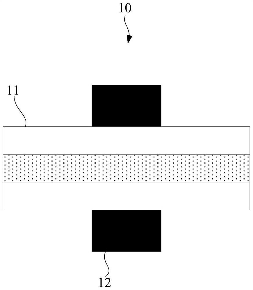
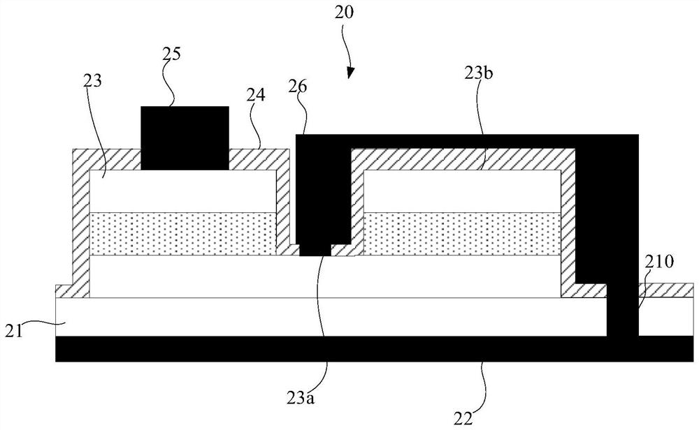
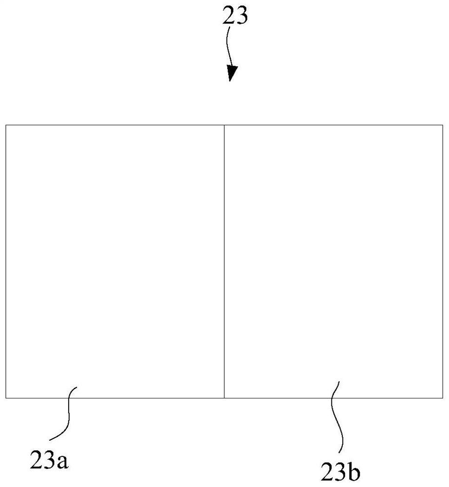
[0054] LED chips can generally be divided into positive structure, flip structure...


PUM


Abstract

The invention relates to a vertical LED chip and a preparation method thereof, an LED array and a display panel. In the vertical LED chip, a conductive layer is arranged on one side, opposite to an epitaxial layer, of a substrate, a through hole is formed in the substrate, and a connecting band can penetrate through a P-type table top and penetrate through the through hole to realize electric connection between an N-type semiconductor layer and the conductive layer, so that the conductive layer is used as an actual N electrode of the vertical LED chip. Under the condition, the N electrode is arranged without stripping the epitaxial layer from the substrate or bonding the epitaxial layer to other substrates, so that the production process of the vertical LED chip is simplified, the production efficiency is improved, the fragment risk caused by the transfer of the epitaxial layer can be avoided, and the production yield of the LED chip is improved.

Description

technical field [0001] The invention relates to the technical field of LEDs, in particular to a vertical LED chip and a preparation method thereof, an LED array and a display panel. Background technique [0002] In the LED chip with vertical structure, because the current can pass through the epitaxial layer evenly when it flows between the two electrodes, so as to avoid the problem of local current congestion and uneven light emission of the epitaxial layer, it has been widely used in actual production. However, the two electrodes in the vertical LED chip are located on both sides of the epitaxial layer, which leads to the fact that when one of the electrodes is prepared, the epitaxial layer must be peeled off from the original substrate and bonded to a new substrate to expose the epitaxial layer. The electrode can only be fabricated after the interface with the original substrate. However, the transfer of the epitaxial layer between the original substrate and the new subs...

Claims


Application Information

Patent Timeline
Patent Type & Authority Applications(China)
IPC IPC(8): H01L33/38H01L33/00H01L33/06H01L33/12
CPCH01L33/382H01L33/12H01L33/06H01L33/005H01L2933/0016
Inventor 戴广超马非凡曹进赵世雄王子川
Owner CHONGQING KONKA PHOTOELECTRIC TECH RES INST CO LTD
Why Eureka
Try Eureka