Cermet vertical pin injection molding process for chip packaging

An injection molding, cermet technology, used in metal processing equipment, transportation and packaging, etc., can solve the problems of high injection molding process cost, low density of packaged parts, poor performance of packaged parts, etc., to eliminate unevenness, improve Hardness and compactness, the effect of improving compactness

Inactive Publication Date: 2020-10-09
株洲天成金属激光高科有限公司
View PDF2 Cites 0 Cited by
  • Summary
  • Abstract
  • Description
  • Claims
  • Application Information

AI Technical Summary

Problems solved by technology

[0002] Integrated circuits that manufacture circuits on the surface of semiconductor chips are also called thin-film integrated circuits; another kind of thick-film integrated circuits is a miniaturized circuit composed of independent semiconductor devices and passive components integrated into substrates or circuit boards. It is necessary to package the chip before it can continue to be used, and the packaging category includes metal packaging, ceramic packaging and plastic packaging, and the injection molding process is generally used for packaging workpieces, which refers to a model with a certain shape, which will be melted by pressure. The colloid in the state is injected into the mold cavity and molded, but most of the existing chip packaging materials are single, which leads to high cost of the injection molding process, and also leads to poor performance of the packaging parts, and the hardness and density are not good during use. High, and in the injection molding process, the degreasing and sintering process is too simple, resulting in low density of packaged parts and poor quality of parts

Method used


Image

  • Cermet vertical pin injection molding process for chip packaging

Examples


Embodiment Construction

[0021] The following will clearly and completely describe the technical solutions in the embodiments of the present invention with reference to the accompanying drawings in the embodiments of the present invention. Obviously, the described embodiments are only some of the embodiments of the present invention, not all of them. Based on the embodiments of the present invention, all other embodiments obtained by persons of ordinary skill in the art without making creative efforts belong to the protection scope of the present invention.

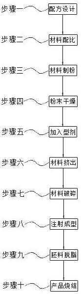
[0022] see figure 1 , the present invention provides a technical solution: a metal ceramic vertical needle injection molding process for chip packaging, comprising the following steps:

[0023] (1) Formula design: design of material formula;

[0024] The ratio of the material formula is carbon: 10.04%-16.04%, peptide: 60.07%-67.07%, nickel 9.00%-11.00%, molybdenum: 7.50%-12.50%, nitrogen: 1.60%-5.20%.

[0025] (2) Ratio of materials: mix titani...


PUM


Abstract

The invention discloses a cermet vertical pin injection molding process for chip packaging. The cermet vertical pin injection molding process for chip packaging comprises the following steps of formula design, material proportioning, material pulverizing, powder drying, addition of a molding agent, material extrusion, material crushing, injection molding, blank degreasing and product sintering. According to the cermet vertical needle injection molding process for chip packaging, a cermet material is adopted, metal can cover the surface of a workpiece after molding, the hardness and the compactness of the workpiece are improved, the production cost is reduced, the compactness of the material is improved through degreasing and sintering, the porosity of the product is reduced, and powder canbe distributed more uniformly by using an adhesive, so that the non-uniformity of the microstructure of a blank can be eliminated, and theoretical density of the workpiece is improved.

Description

technical field [0001] The invention relates to the technical field of injection molding, in particular to a cermet vertical needle injection molding process for chip packaging. Background technique [0002] Integrated circuits that manufacture circuits on the surface of semiconductor chips are also called thin-film integrated circuits; another kind of thick-film integrated circuits is a miniaturized circuit composed of independent semiconductor devices and passive components integrated into substrates or circuit boards. It is necessary to package the chip before it can continue to be used, and the packaging category includes metal packaging, ceramic packaging and plastic packaging, and the injection molding process is generally used for packaging workpieces, which refers to a model with a certain shape, which will be melted by pressure. The colloid in the state is injected into the mold cavity and molded, but most of the existing chip packaging materials are single, which l...

Claims


Application Information

Patent Timeline
Patent Type & Authority Applications(China)
IPC IPC(8): C22C29/02C22C1/05B22F3/22B22F1/00B22F3/10B22F3/15
CPCC22C29/02C22C1/051B22F3/225B22F3/227B22F3/1021B22F3/15B22F2998/10B22F1/10
Inventor 王受杨
Owner 株洲天成金属激光高科有限公司
Why Eureka
Try Eureka