Novel multilayer tunneling junction and application thereof in double-junction laminated battery
A tunneling junction, a new type of technology, applied in circuits, photovoltaic power generation, electrical components, etc., can solve the problems of poor performance of heterojunction batteries, poor performance of transparent conductive films, and reduced battery performance, and achieve high thermal stability. Effect
- Summary
- Abstract
- Description
- Claims
- Application Information
AI Technical Summary
Problems solved by technology
Method used
Image
Examples
Embodiment 1
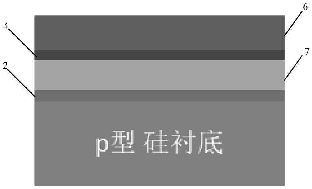
[0045] A silicon oxide layer with a thickness of less than 5nm, that is, the first ultra-thin dielectric layer 2, is prepared on a p-type silicon substrate by wet chemical oxidation, high temperature oxidation or plasma-assisted oxidation, and is prepared on it by PECVD and other thin film deposition equipment A layer of p-type heavily doped silicon film 7 precursor with a thickness of 5-200nm, followed by annealing at a high temperature of 500-1100°C to obtain the first layer of heavily-doped silicon film layer, and then prepare the second layer on top by the same method Ultra-thin dielectric layer 4 and a layer of n-type heavily doped silicon thin film 6 precursors with a thickness of 5-200nm, followed by annealing the second heavily doped silicon thin film layer by rapid annealing (annealing temperature is 600-1000°C) . The prepared tunneling junction based on crystalline silicon bottom cell is as follows figure 2 As shown, the contact resistivity is about 0.01mΩ·cm2, and...
Embodiment 2
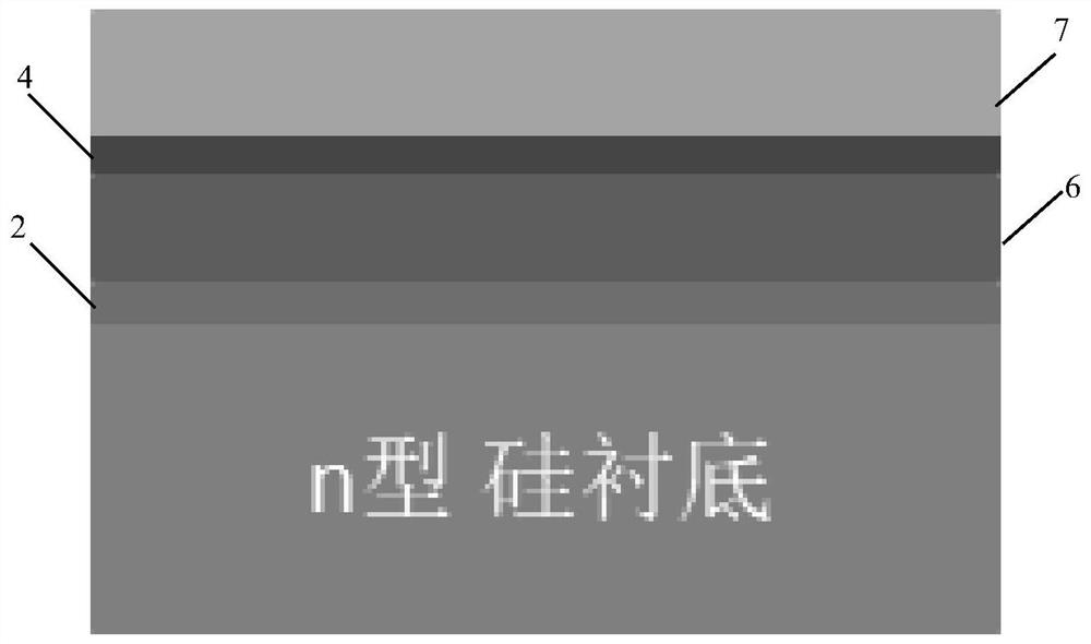
[0047] A silicon oxide layer with a thickness of less than 5nm, that is, the first ultra-thin dielectric layer 2, is prepared on the n-type silicon substrate by wet chemical oxidation, high temperature oxidation or plasma-assisted oxidation, and is prepared on it with thin film deposition equipment such as PECVD. A layer of n-type heavily doped silicon thin film 6 precursor with a thickness of 5-200nm, followed by annealing at a high temperature of 500-1100°C to obtain the first heavily doped silicon thin film layer, and then prepare the second layer on top by the same method An ultra-thin dielectric layer 4 and a p-type heavily doped silicon thin film 7 precursor with a thickness of 5-200nm, followed by annealing the second heavily doped silicon thin film layer by rapid annealing (the annealing temperature is 600-1000°C) . The prepared tunneling junction based on crystalline silicon bottom cell is as follows image 3 As shown, the contact resistivity is about 0.01mΩ·cm2, and...
Embodiment 3
[0049] Under certain conditions, the preparation of the tunnel junction structure can also be realized by omitting the second ultra-thin dielectric layer 4: on the p-type silicon substrate, a layer with a thickness of less than The 5nm silicon oxide layer is the first ultra-thin dielectric layer 2, and a p-type heavily doped silicon thin film 7 precursor with a thickness of 5-200nm is prepared on it with a thin film deposition equipment such as PECVD, and then heated at a high temperature of 500-1100°C Perform annealing to obtain the first layer of heavily doped silicon thin film layer, omit the second ultra-thin dielectric layer 4, directly prepare a layer of n-type heavily doped silicon thin film 6 precursor with a thickness of 5-200nm, and then use the method of rapid annealing Annealing the second heavily doped silicon thin film layer (annealing temperature is 600-1000°C). The prepared tunneling junction based on crystalline silicon bottom cell is as follows Figure 4 As ...
PUM
| Property | Measurement | Unit |
|---|---|---|
| thickness | aaaaa | aaaaa |
| thickness | aaaaa | aaaaa |
| thickness | aaaaa | aaaaa |
Abstract
Description
Claims
Application Information
 - R&D Engineer
- R&D Manager
- IP Professional
- Industry Leading Data Capabilities
- Powerful AI technology
- Patent DNA Extraction
Browse by: Latest US Patents, China's latest patents, Technical Efficacy Thesaurus, Application Domain, Technology Topic, Popular Technical Reports.
© 2024 PatSnap. All rights reserved.Legal|Privacy policy|Modern Slavery Act Transparency Statement|Sitemap|About US| Contact US: help@patsnap.com


