A double-strip silicon nitride waveguide and its preparation method

A technology of silicon nitride wave and silicon nitride, applied in the direction of optical waveguide light guide, light guide, instrument, etc., can solve the problem of low verticality, achieve the effect of improving verticality, avoiding process errors, and reducing impact

Active Publication Date: 2021-02-09
GUIYANG UNIV
View PDF5 Cites 0 Cited by
  • Summary
  • Abstract
  • Description
  • Claims
  • Application Information

AI Technical Summary

Problems solved by technology

[0012] In order to solve the above-mentioned technical problems, one of the objects of the present invention is to provide a double-strip silicon nitride waveguide, which forms a vertical double-strip waveguide structure, which solves the problem of directly etching the dielectric material SiO2 in the traditional process. 2 The problem of low verticality

Method used


Image

  • A double-strip silicon nitride waveguide and its preparation method
  • A double-strip silicon nitride waveguide and its preparation method
  • A double-strip silicon nitride waveguide and its preparation method

Examples


Embodiment 1

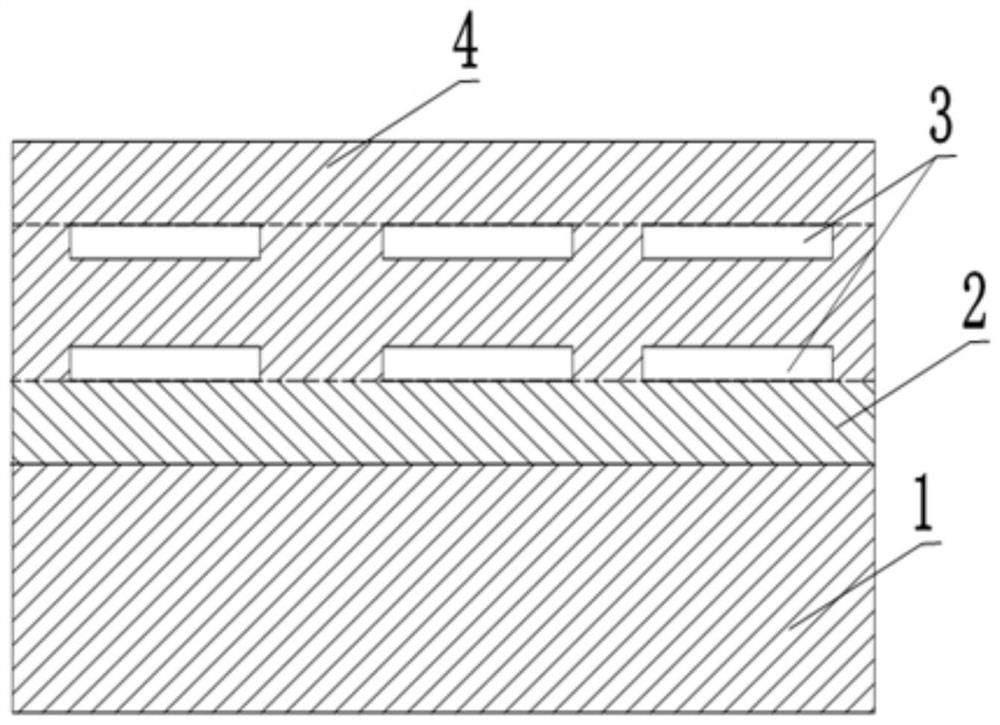
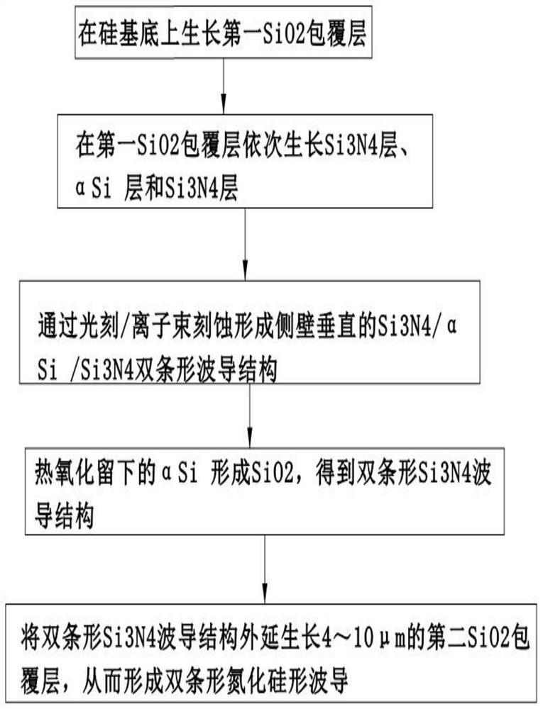
[0059] A dual strip silicon nitride waveguide comprising:

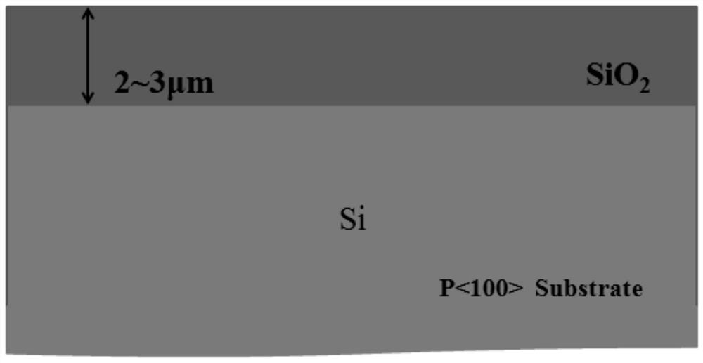
[0060] Silicon substrate 1;

[0061] The first SiO uniformly covered on the upper surface of the silicon substrate 2 cladding layer 2; the first SiO 2 The thickness of the cladding layer is 2-3 μm;

[0062] Located on the first SiO 2 Bistripe Si on the upper surface of the cladding 3 N 4 waveguide structure 3; the double-strip Si 3 N 4 Each Si of the waveguide structure 3 N 4 The thickness of the waveguide structure is 100-250nm; the double strip Si 3 N 4 The sidewall of the waveguide structure is perpendicular to the silicon substrate, and the double-striped Si 3 N 4 The upper and lower two Si of the waveguide structure 3 N 4 The corresponding sidewalls of the waveguide structure are aligned with each other; the double-strip Si 3 N 4 The waveguide structure is a vertically symmetrical structure with a pitch of 400nm-1.5μm.

[0063] The double bar Si 3 N 4 The waveguide structure is covered by a sec...


PUM

PropertyMeasurementUnit
thicknessaaaaaaaaaa
thicknessaaaaaaaaaa
thicknessaaaaaaaaaa

Abstract

The invention discloses a double-strip silicon nitride waveguide and a preparation method thereof. The waveguide comprises: a silicon substrate; a first SiO layer uniformly covered on the upper surface of the silicon substrate; 2 cladding layer; located on the first SiO 2 Bistripe Si on the upper surface of the cladding 3 N 4 waveguide structure; the double-strip Si 3 N 4 The waveguide structure is covered by a second SiO 2 The cladding layer wraps; its preparation process forms the first SiO2 on the silicon substrate by thermal oxygen process 2 cladding layer; sequential growth of Si 3 N 4 layer / αSi layer / Si 3 N 4 layer; αSi / Si formed by photolithography / ion beam etching 3 N 4 Double-strip silicon nitride waveguide structure; wet etching is used to partially remove the αSi material in the interlayer, and the high temperature oxidation resistance of silicon nitride material is used to thermally oxidize the remaining αSi to form SiO 2 ; Finally, the second SiO is grown by PECVD process 2 The cladding layer is used to produce a double-strip silicon nitride waveguide.

Description

technical field [0001] The invention relates to the technical field of optical materials, in particular to a double-strip silicon nitride waveguide and a preparation method thereof. Background technique [0002] An optical waveguide is a dielectric device that guides light waves to propagate in it, also known as a dielectric optical waveguide. Among them, silica waveguide is a very common and important kind of PLC optical waveguide material, which is generally prepared by planar optical waveguide technology. [0003] The manufacturing process of conventional silica optical waveguide is as follows: [0004] 1) Use flame hydrolysis (FHD) or chemical vapor deposition (CVD) to grow a layer of SiO on the silicon wafer 2 , which is doped with phosphorus and boron ions as the lower cladding of the waveguide; [0005] 2) Use FHD or CVD process to grow another layer of SiO on the lower cladding layer 2 , as a waveguide core layer, which is doped with germanium ions to obtain the ...

Claims


Application Information

Patent Timeline
Patent Type & Authority Patents(China)
IPC IPC(8): G02B6/122G02B6/136G02B6/13
CPCG02B6/122G02B6/13G02B6/131G02B6/136G02B2006/12035G02B2006/12166G02B2006/12178
Inventor 周章渝肖寒孙健代天军陈雨青彭晓珊王代强张青竹宁江华张子砚
Owner GUIYANG UNIV
Why Eureka
Try Eureka