Chuck structure and semiconductor manufacturing apparatus including the same

A technology for manufacturing equipment and semiconductors, applied in semiconductor/solid-state device manufacturing, electrical components, circuits, etc., can solve problems such as interference, and achieve the effect of preventing process errors and improving efficiency

Pending Publication Date: 2022-04-08
SK HYNIX INC
View PDF1 Cites 0 Cited by
  • Summary
  • Abstract
  • Description
  • Claims
  • Application Information

AI Technical Summary

Problems solved by technology

In addition, since the chuck can pick up semiconductor chips one by one, interference may occur between the semiconductor chip picked up by the chuck and adjacent semiconductor chips or other parts

Method used


Image

  • Chuck structure and semiconductor manufacturing apparatus including the same
  • Chuck structure and semiconductor manufacturing apparatus including the same
  • Chuck structure and semiconductor manufacturing apparatus including the same

Examples


Embodiment Construction

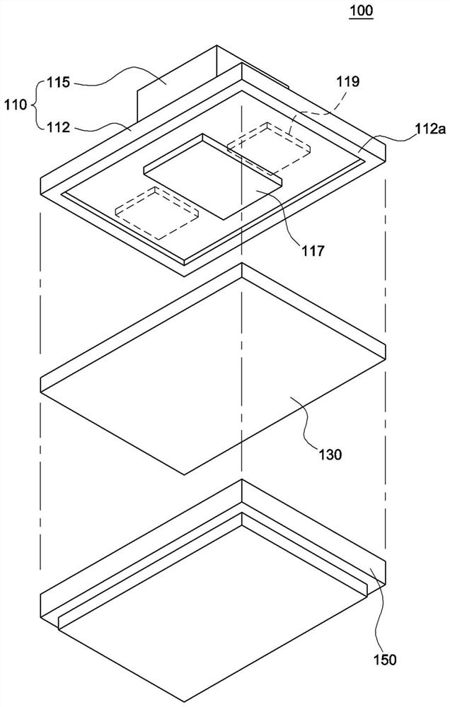
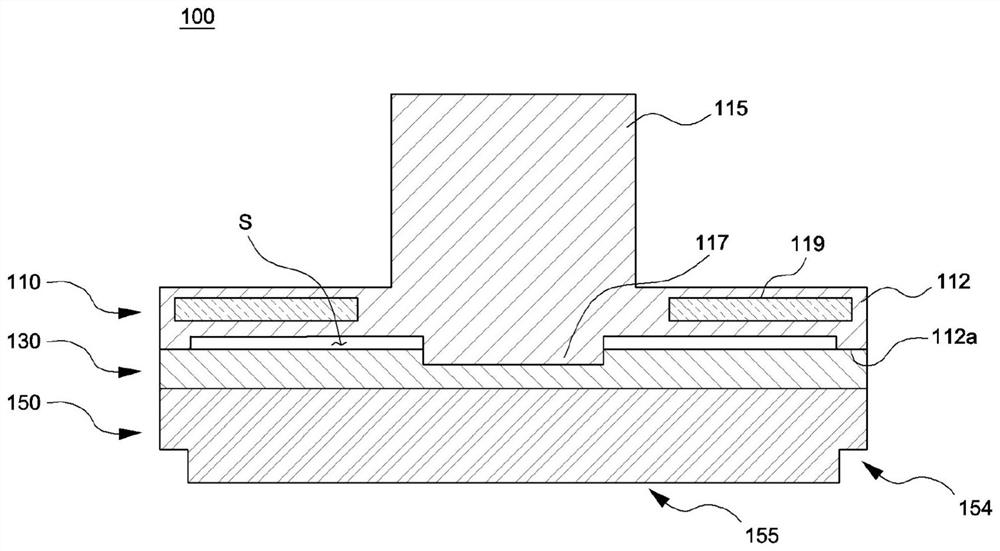
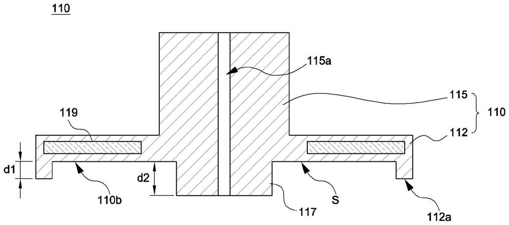
[0024] Various embodiments of the invention will be described in more detail with reference to the accompanying drawings. The Figures are schematic illustrations of various embodiments and intermediate structures. Likewise, variations in the configuration and shape of the illustrations as a result, for example, of manufacturing techniques and / or tolerances are contemplated. Accordingly, the described embodiments should not be construed as limited to the specific configurations and shapes shown herein but may include deviations in configurations and shapes without departing from the spirit and scope of the present invention as defined in the appended claims.

[0025] The invention is described herein with reference to cross-sectional and / or plan illustrations of embodiments of the invention. However, the embodiments of the present invention should not be construed as limiting the concept of the present invention. While a few embodiments of the present invention will be shown ...


PUM

PropertyMeasurementUnit
thicknessaaaaaaaaaa

Abstract

The invention provides a chuck structure and a semiconductor manufacturing apparatus including the same. A semiconductor manufacturing apparatus may include a chuck structure configured to pick up a semiconductor chip. The collet structure may include a holder, a plate, an attraction member, and an edge contact portion. The holder may be configured to receive the vacuum downward. The holder may include a magnet disposed in the holder. The plate may include an upper surface magnetically and mechanically coupled with the holder. The plate may include sidewalls fully exposed by the holder. The plate may receive a vacuum from the holder. The suction member may be in contact with the plate to pick up the semiconductor chip using a vacuum received from the plate. The edge contact portion may include a protruding portion having a first length protruding from an edge portion of a bottom surface of the holder to contact the plate.

Description

technical field [0001] Various embodiments of the present invention relate generally to semiconductor manufacturing systems, and more particularly to chuck structures for semiconductor chip pick-up. Various embodiments of the present invention also relate to semiconductor fabrication equipment including collet structures. Background technique [0002] Generally, semiconductor devices can be integrated on a semiconductor substrate by repeatedly performing a series of semiconductor manufacturing processes. A semiconductor substrate (ie, a semiconductor wafer) may include a plurality of semiconductor chips or semiconductor dies. After the semiconductor manufacturing process is completed, the semiconductor substrate may be singulated into semiconductor chips. A process of dividing a semiconductor chip may be referred to as a dicing process. Segmented semiconductor chips may be bonded to a packaging substrate. [0003] A semiconductor chip separated from a semiconductor subst...

Claims


Application Information

Patent Timeline
Patent Type & Authority Applications(China)
IPC IPC(8): H01L21/683
CPCH01L21/6838H01L21/67144H01L21/67721H05K13/0404H01L21/68778
Inventor 禹仲范金秀赫李炳昊林泰焕
Owner SK HYNIX INC
Why Eureka
Try Eureka