Double-strip-shaped silicon nitride waveguide and preparation method thereof
A technology of silicon nitride wave and silicon nitride, which is applied in the field of double-strip silicon nitride waveguide and its preparation, can solve the problem of low verticality, achieve the effects of improving verticality, avoiding process errors, and reducing absorption loss
- Summary
- Abstract
- Description
- Claims
- Application Information
AI Technical Summary
Problems solved by technology
Method used
Image

Examples
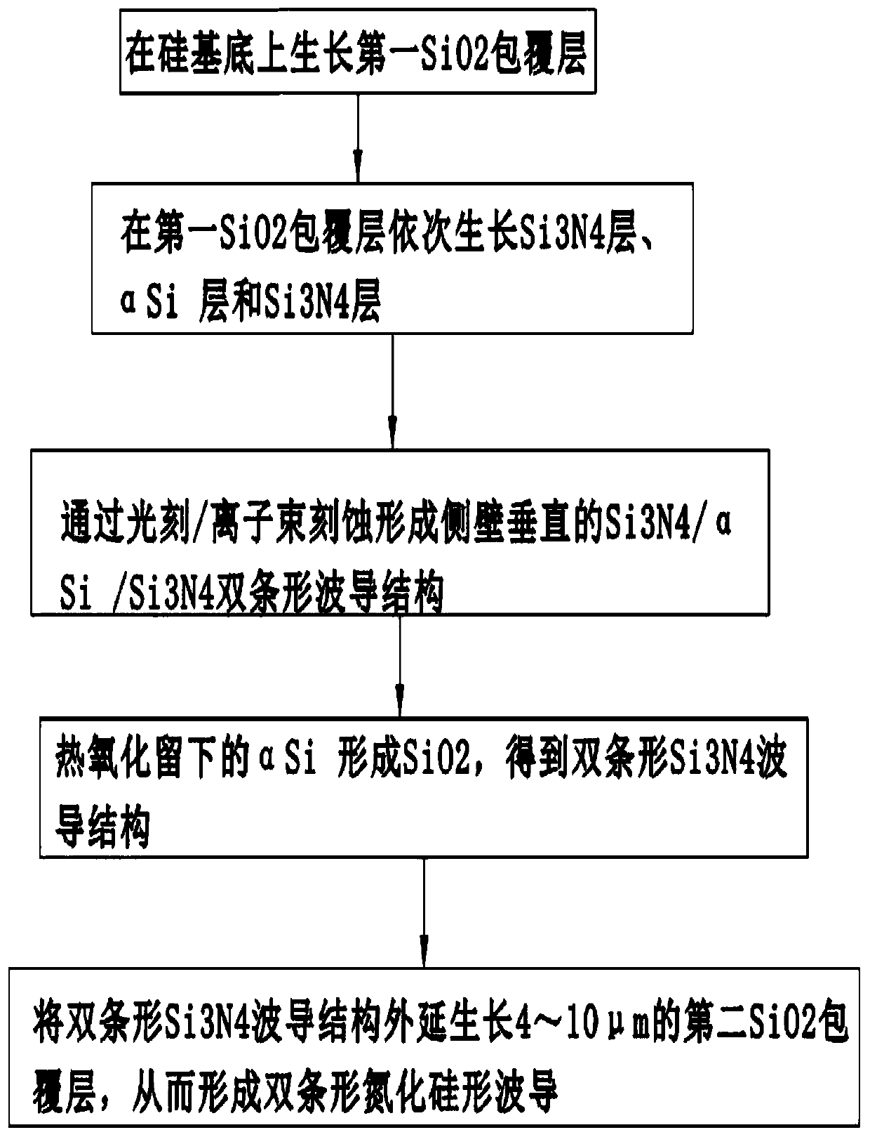
Embodiment 1
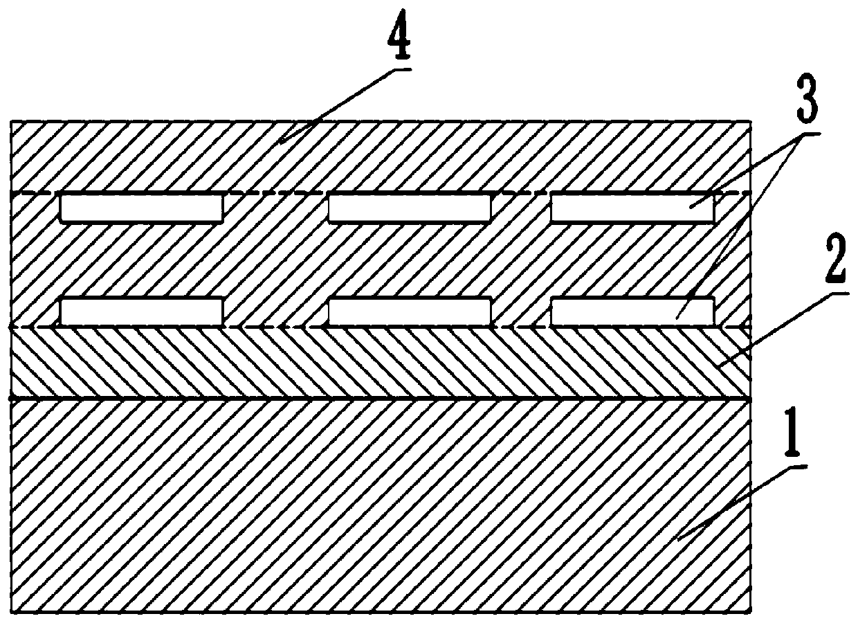
[0059] A dual strip silicon nitride waveguide comprising:
[0060] Silicon substrate 1;
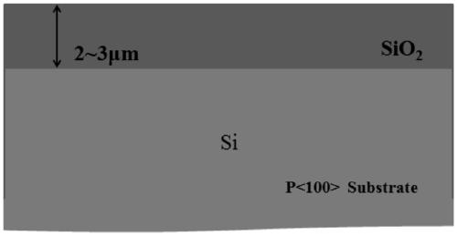
[0061] The first SiO uniformly covered on the upper surface of the silicon substrate 2 cladding layer 2; the first SiO 2 The thickness of the cladding layer is 2-3 μm;
[0062] Located on the first SiO 2 Bistripe Si on the upper surface of the cladding 3 N 4 waveguide structure 3; the double-strip Si 3 N 4 Each Si of the waveguide structure 3 N 4 The thickness of the waveguide structure is 100-250nm; the double strip Si 3 N 4 The sidewall of the waveguide structure is perpendicular to the silicon substrate, and the double-striped Si 3 N 4 The upper and lower two Si of the waveguide structure 3 N 4 The corresponding sidewalls of the waveguide structure are aligned with each other; the double-strip Si 3 N 4 The waveguide structure is a vertically symmetrical structure with a pitch of 400nm-1.5μm.
[0063] The double bar Si 3 N 4 The waveguide structure is covered by a sec...
PUM
| Property | Measurement | Unit |
|---|---|---|
| thickness | aaaaa | aaaaa |
| thickness | aaaaa | aaaaa |
| thickness | aaaaa | aaaaa |
Abstract
Description
Claims
Application Information
 - R&D
- Intellectual Property
- Life Sciences
- Materials
- Tech Scout
- Unparalleled Data Quality
- Higher Quality Content
- 60% Fewer Hallucinations
Browse by: Latest US Patents, China's latest patents, Technical Efficacy Thesaurus, Application Domain, Technology Topic, Popular Technical Reports.
© 2025 PatSnap. All rights reserved.Legal|Privacy policy|Modern Slavery Act Transparency Statement|Sitemap|About US| Contact US: help@patsnap.com