A box-shaped silicon nitride waveguide and its preparation method

A technology for forming silicon nitride and silicon nitride, which is applied in the field of BOX-shaped silicon nitride waveguide and its preparation, and can solve the problems of inconvenient, uneven bottom and side, and low verticality

Active Publication Date: 2021-01-19
GUIYANG UNIV
View PDF11 Cites 0 Cited by
  • Summary
  • Abstract
  • Description
  • Claims
  • Application Information

AI Technical Summary

Problems solved by technology

However, the side walls obtained by directly digging grooves on silicon dioxide are not steep enough, the verticality is not high, the bottom and sides are not flat enough, and most of the groove depth is controlled by RIE etching technology, which requires the width of the groove
In addition, when the thickness of the silicon nitride optical waveguide needs to be changed, the production and preparation process needs to be readjusted, which takes a lot of time and is very inconvenient

Method used


Image

  • A box-shaped silicon nitride waveguide and its preparation method
  • A box-shaped silicon nitride waveguide and its preparation method
  • A box-shaped silicon nitride waveguide and its preparation method

Examples


Embodiment 1

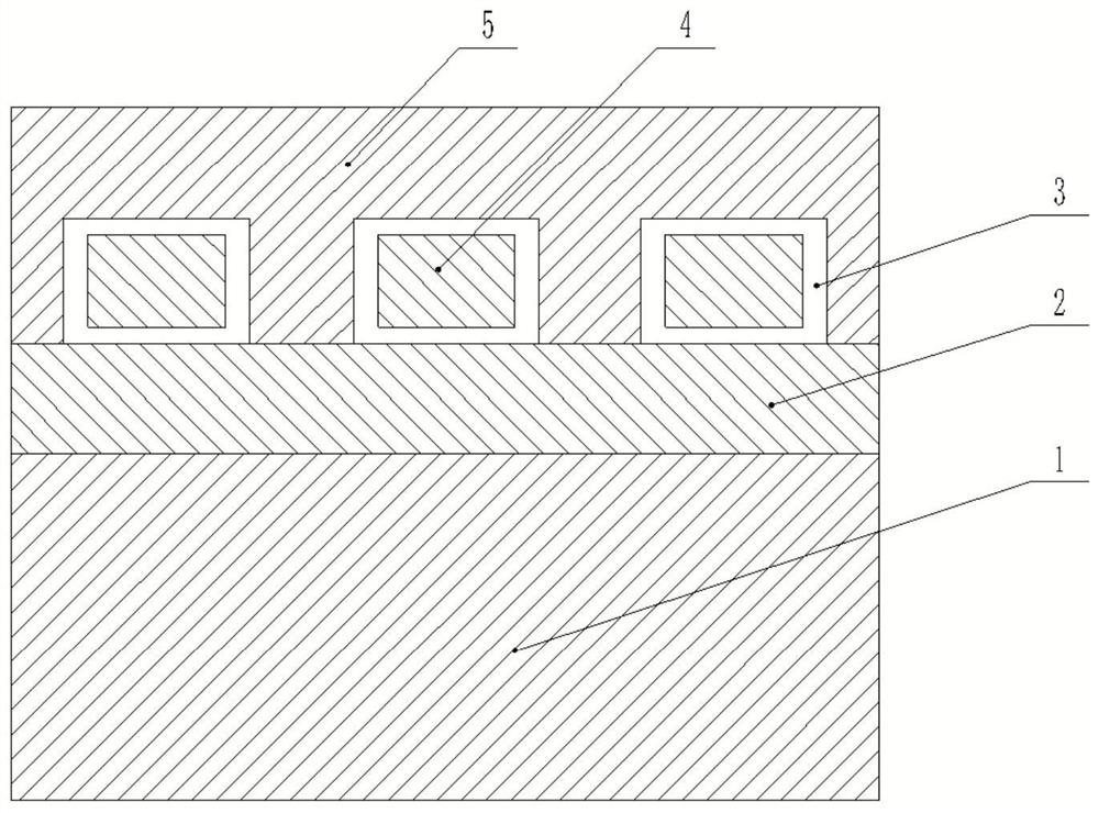
[0053] Such as figure 1 As shown, a BOX-shaped silicon nitride waveguide includes:

[0054] A first cladding layer 2 located on the semiconductor substrate 1;

[0055] and a BOX silicon nitride waveguide 3 located on the first cladding layer 2; and a second cladding layer 4 located inside the BOX silicon nitride waveguide 3;

[0056] and a third cladding layer 5 located on the first cladding layer 2 and covering the BOX silicon nitride waveguide 3;

[0057] The first cladding layer 2, the second cladding layer 4 and the third cladding layer 5 comprise silicon dioxide;

[0058] The semiconductor substrate 1 is a silicon substrate;

[0059] The thickness of the first coating layer 2 is 3 μm; the thickness of the third coating layer 5 is 7 μm.

[0060] The method for preparing the BOX-shaped silicon nitride waveguide of this embodiment includes the following steps:

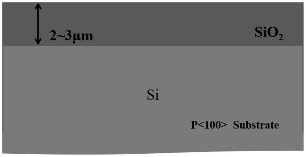
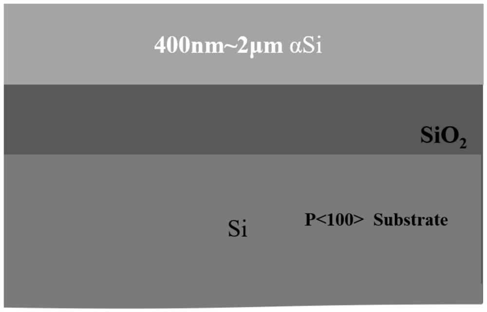
[0061] S1. If Figure 2-4 As shown, a 3 μm thick SiO was grown on a silicon substrate using thermal oxygen ...

Embodiment 2

[0078] Such as figure 1 As shown, a BOX-shaped silicon nitride waveguide includes:

[0079] A first cladding layer 2 located on the semiconductor substrate 1;

[0080] and a BOX silicon nitride waveguide 3 located on the first cladding layer 2; and a second cladding layer 4 located inside the BOX silicon nitride waveguide 3;

[0081] and a third cladding layer 5 located on the first cladding layer 2 and covering the BOX silicon nitride waveguide 3;

[0082] The first cladding layer 2, the second cladding layer 4 and the third cladding layer 5 comprise silicon dioxide;

[0083] The semiconductor substrate 1 is a silicon substrate;

[0084] The thickness of the first cladding layer 2 is 2 μm; the thickness of the third cladding layer 5 is 5 μm.

[0085] The method for preparing the BOX-shaped silicon nitride waveguide of this embodiment includes the following steps:

[0086] S1. If Figure 2-4 As shown, 2 μm thick SiO was grown on a silicon substrate using thermal oxygen ...


PUM

PropertyMeasurementUnit
thicknessaaaaaaaaaa
thicknessaaaaaaaaaa
thicknessaaaaaaaaaa

Abstract

The invention discloses a BOX-shaped silicon nitride waveguide and a preparation method thereof, belonging to the technical field of optical materials. The method comprises: sequentially forming a first cladding layer, a first sacrificial layer and a second sacrificial layer on a semiconductor substrate; The first sacrificial layer and the second sacrificial layer are etched, the second sacrificial layer is removed, and a strip-shaped groove is formed; a part of the silicon nitride material is grown in the strip-shaped groove, and a part is covered on the first sacrificial layer, and the surface is flattened. Form the BOX silicon nitride groove; grow the second cladding layer, partially fill the BOX silicon nitride groove, and partially cover the first sacrificial layer, the surface is flattened to form a smooth surface; the silicon nitride material is grown to cover the smooth surface; The silicon nitride material outside the BOX silicon nitride groove is etched to form the BOX silicon nitride waveguide, and the first sacrificial layer is etched; the third cladding layer is grown on the first cladding layer and the BOX silicon nitride waveguide, which solves the problem. The traditional process directly etchs the dielectric material SiO 2 The problem of low verticality.

Description

technical field [0001] The invention relates to the technical field of optical materials, in particular to a BOX-shaped silicon nitride waveguide and a preparation method thereof. Background technique [0002] An optical waveguide is a dielectric device that guides light waves to propagate in it, also known as a dielectric optical waveguide. Dielectric waveguides are the basic structural units of integrated optical systems and their components. The dielectric waveguide mainly plays the role of confinement, transmission and coupling of light waves. Dielectric waveguides can be divided into four categories according to the cross-sectional shape: cylindrical waveguides (optical fibers), film (planar) waveguides, rectangular (strip) waveguides and ridge waveguides. Thin-film waveguides and rectangular waveguides (BOX waveguides) are commonly used in integrated optics. There are many types of materials used to form optical waveguides, and silicon nitride is currently a commonl...

Claims


Application Information

Patent Timeline
Patent Type & Authority Patents(China)
IPC IPC(8): G02B6/122G02B6/13G02B6/136
CPCG02B6/122G02B6/13G02B6/136G02B2006/12035G02B2006/12166G02B2006/12176
Inventor 周章渝肖寒孙健代天军陈雨青彭晓珊王代强张青竹宁江华张子砚
Owner GUIYANG UNIV
Why Eureka
Try Eureka