
Method of establishing optical data correction model

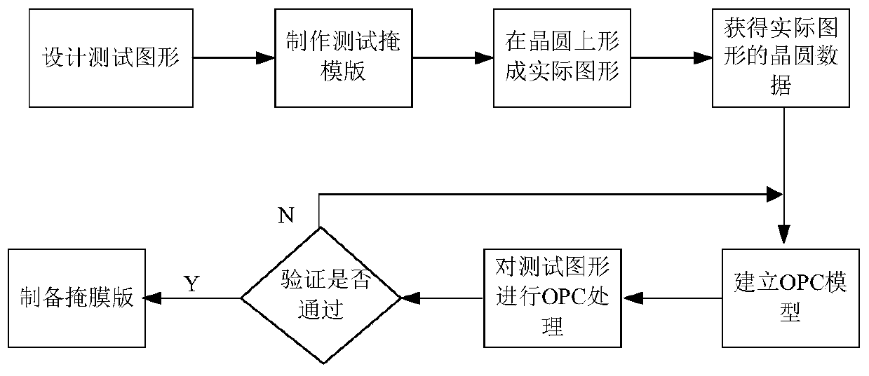
A model and data technology, applied in the field of building OPC models, can solve the problems of low overall efficiency and time-consuming, and achieve the effect of ensuring accuracy, shortening modeling time, and improving R&D efficiency.

Active Publication Date: 2020-07-17
NEXCHIP SEMICON CO LTD
View PDF5 Cites 3 Cited by
  • Summary
  • Abstract
  • Description
  • Claims
  • Application Information

AI Technical Summary

Problems solved by technology

In the prior art, the wafer data required for OPC processing is obtained manually by using a scanning electron microscope (CDSEM) for feature size measurement, which takes a lot of time and the overall efficiency is low

Method used


Image

  • Method of establishing optical data correction model
  • Method of establishing optical data correction model
  • Method of establishing optical data correction model

Examples


Embodiment Construction

[0035] The method for establishing the OPC model of the present invention will be further described in detail below in conjunction with the accompanying drawings and specific embodiments. According to the following description and accompanying drawings, the advantages and characteristics of the present invention will be clearer, however, it should be noted that the concept of the technical solution of the present invention can be implemented in many different forms, and is not limited to the specific implementation set forth herein. example. The drawings are all in very simplified form and use imprecise scales, and are only used to facilitate and clearly assist the purpose of illustrating the embodiments of the present invention.

[0036] The terms "first", "second", etc. in the specification are used to distinguish between similar elements, and are not necessarily used to describe a specific order or chronological order. It is to be understood that the terms so used are inte...


PUM


Abstract

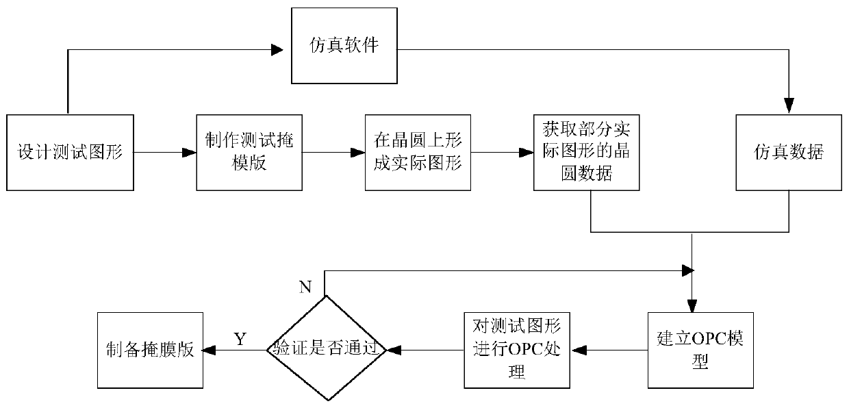
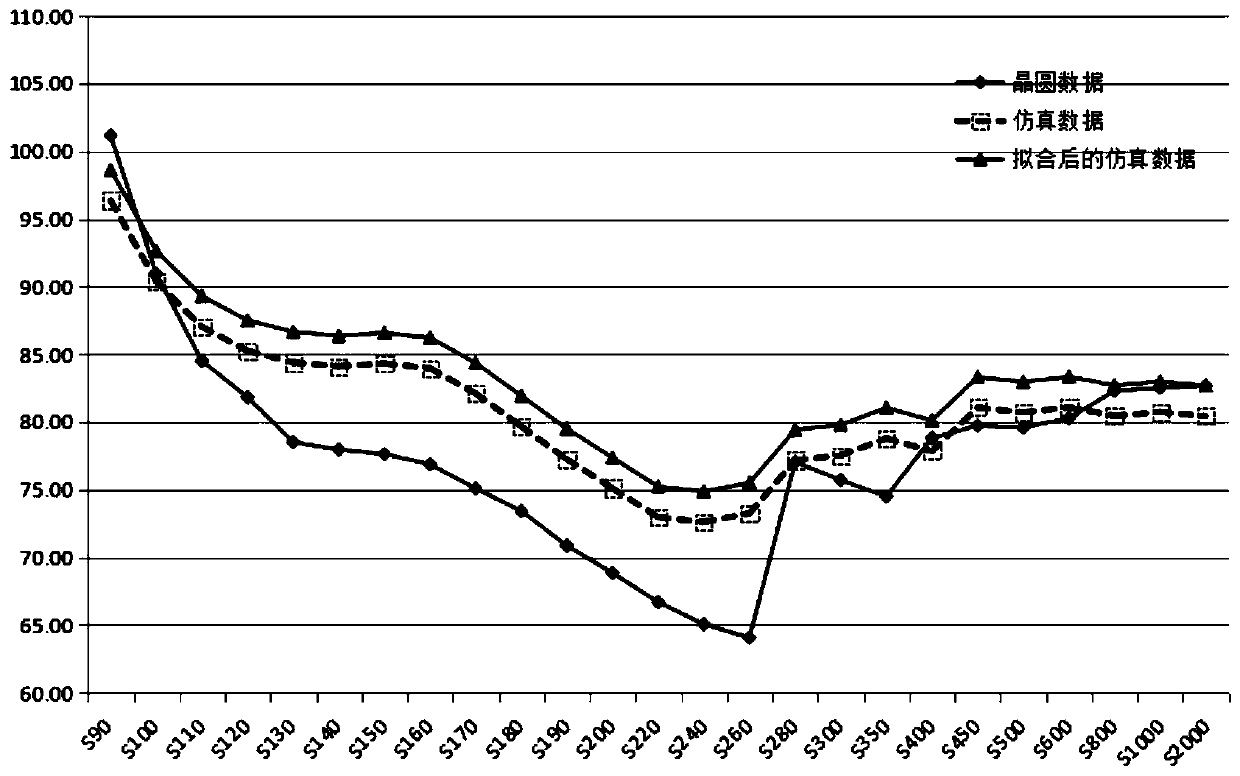
The invention provides a method for establishing an OPC model. The method comprises the following steps of transferring a test graph to a wafer by using a test mask plate; forming an actual graph on awafer, obtaining the wafer data obtained by testing part of the actual graph, simulating the test graph through a simulation software to obtain the simulation data of the test graph, fitting the simulation data with the wafer data, and establishing an OPC model by adopting the fitted simulation data. According to the method for establishing the OPC model provided by the invention, the wafer dataof part of the actual graph is fitted with the overall simulation data of the test graph, and the OPC model is established through the fitted data, so that the situation of spending a lot of time to obtain the large amount of wafer data is avoided, the modeling time is shortened, and the research and development efficiency is improved.

Description

technical field [0001] The invention relates to the technical field of integrated circuit optical data processing, in particular to a method for establishing an OPC model. Background technique [0002] With the continuous development of integrated circuits and the continuous development of manufacturing technology towards smaller dimensions, the photolithography process has become the main bottleneck restricting the development of integrated circuits to smaller feature sizes. In the deep submicron semiconductor manufacturing process, the feature size is already far smaller than the wavelength of the light source. Due to the nature of light waves and the problems of the actual projection exposure system, there will be serious energy loss caused by limited diffraction or nonlinear filtering of the imaging system. That is, the Optical Proximity Effect (OPE), which will inevitably lead to distortions in the process of transferring the pattern on the mask to the wafer, such as co...

Claims


Application Information

Patent Timeline
IPC IPC(8): G03F7/20G06F30/20
CPCG03F7/70441G03F7/705
Inventor 王康罗招龙
Owner NEXCHIP SEMICON CO LTD
Learn More