Preparation method, product and application of a two-dimensional ndocl single crystal material
A single crystal material and powder technology, which is applied in the field of preparation of two-dimensional NdOCl single crystal material, can solve the problems of unfriendly environment and poor stability, and achieve the effects of improved sensitivity, high breakdown voltage and improved resolution
- Summary
- Abstract
- Description
- Claims
- Application Information
AI Technical Summary
Problems solved by technology
Method used
Image
Examples
preparation example Construction
[0035] In one aspect, the present invention provides a two-dimensional NdOCl single crystal material and a preparation method thereof, the specific implementation steps are as follows:
[0036] Step 1: Add NdCl 3 ·6H 2O is ground into powder, placed in a muffle furnace and heated to 500-900°C, kept for 12-24 hours, and calcined to obtain NdOCl powder;
[0037] Step 2: Mix the NdOCl powder and flux obtained in step 1 with a mass ratio of 1:1 to 5:1 as a precursor and place it in a porcelain boat, and place the porcelain boat loaded with the precursor in a horizontal tube furnace The central temperature zone, the substrate is placed in the central temperature zone or the downstream temperature zone, the flux is chloride salt, and the substrate is any one of doped silicon wafers with oxide layers, mica sheets, and sapphire ;
[0038] Step 3: Introduce argon gas into the tube furnace, and maintain the gas flow rate of 50-200 sccm, heat the central temperature zone to 700-1000° ...
Embodiment 1
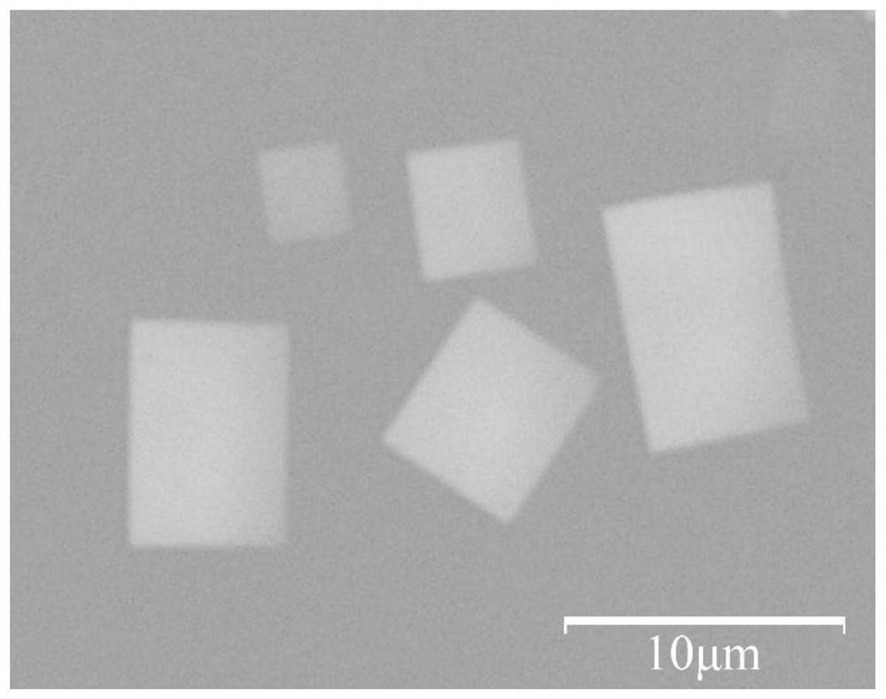
[0046] According to the method for preparing a two-dimensional NdOCl single crystal material provided by the present invention, a horizontal tube furnace is used, 100 mg of NdOCl powder, 50 mg of chloride salt (such as NaCl), sapphire substrate, a central temperature zone of 750 ° C, and a holding time of 30 min. Pre-evacuation was carried out before the reaction, and then Ar gas was charged to an atmospheric pressure, and a gas flow rate of 500 sccm was kept for 5 minutes to wash the gas. After the reaction, the carrier gas remains unchanged, the product is cooled to room temperature with the furnace, and the product is collected on the sapphire substrate to obtain a two-dimensional NdOCl single crystal material with a nanosheet structure.
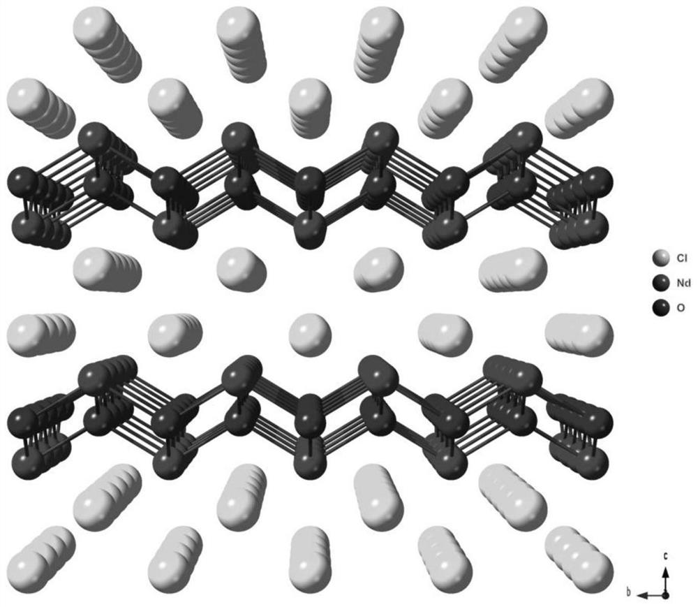
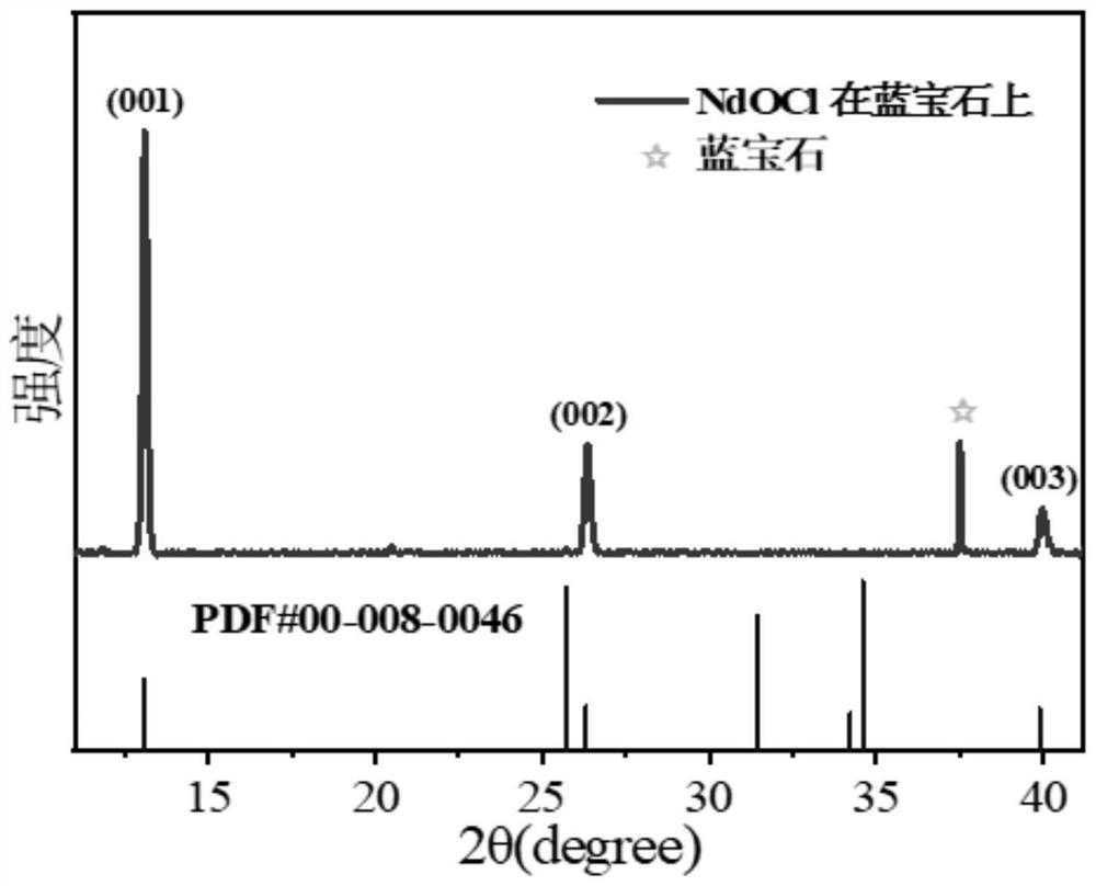
[0047] figure 1 It is a schematic structural diagram of the two-dimensional NdOCl single crystal material prepared in Example 1, and the crystal layers of the two-dimensional NdOCl single crystal material are connected by van der Waals fo...
Embodiment 2
[0052] According to the preparation method of a two-dimensional material X-ray detector provided by the present invention, the two-dimensional NdOCl single crystal material is prepared in Example 1 and transferred to the substrate. The substrate adopts a doped silicon wafer with an oxide layer. Thermal evaporation deposited 10 nm chromium and 90 nm gold as electrodes. X-rays are irradiated vertically on the surface of the two-dimensional material, and a bias voltage is applied to both ends of the electrodes to test the photocurrent and dark current.
[0053] Image 6 It is a structural schematic diagram of the X-ray detector prepared in Example 2. The two-dimensional NdOCl single crystal material is placed on the surface of the doped silicon wafer with an oxide layer, and a pair of Au / Cr counter electrodes are deposited on the upper surface of the two-dimensional NdOCl single crystal material. .
[0054] Figure 7 It is the current-voltage curve diagram before and after add...
PUM
| Property | Measurement | Unit |
|---|---|---|
| thickness | aaaaa | aaaaa |
| thickness | aaaaa | aaaaa |
| thickness | aaaaa | aaaaa |
Abstract
Description
Claims
Application Information
 - R&D Engineer
- R&D Manager
- IP Professional
- Industry Leading Data Capabilities
- Powerful AI technology
- Patent DNA Extraction
Browse by: Latest US Patents, China's latest patents, Technical Efficacy Thesaurus, Application Domain, Technology Topic, Popular Technical Reports.
© 2024 PatSnap. All rights reserved.Legal|Privacy policy|Modern Slavery Act Transparency Statement|Sitemap|About US| Contact US: help@patsnap.com


