ESD protection structure, integrated circuit and electronic equipment

An ESD protection, integrated circuit technology, applied in emergency protection circuit devices, emergency protection circuit devices for limiting overcurrent/overvoltage, circuits, etc. Comprehensive and other issues, to achieve the effect of improving the response speed of ESD protection, protecting internal circuits, and reducing power consumption

Active Publication Date: 2020-07-03
INST OF MICROELECTRONICS CHINESE ACAD OF SCI
View PDF5 Cites 0 Cited by
  • Summary
  • Abstract
  • Description
  • Claims
  • Application Information

AI Technical Summary

Problems solved by technology

A defect in the general SCR device structure diagram is that the trigger voltage is too high
The trigger voltage of a simple SCR is equivalent to the reverse breakdown voltage of a PN junction formed by an N-well and a P-well, generally between a dozen volts and tens of volts. Such a high breakdown voltage cannot provide effective ESD protection for internal circuit components. , because before the SCR is turned on, the internal components have been damaged by the ESD pulse voltage
[0004] Moreover, in the existing chip protection schemes, the ESD protection circuit design is generally only added at the input and output terminals, and the ESD between VDD and VSS is generally ignored Protection design, causing abnormal damage inside the chip
[0005]That is to say, the ESD protection of integrated circuits in the prior art has the technical problems of incomplete protection circuit and slow protection response

Method used


Image

  • ESD protection structure, integrated circuit and electronic equipment
  • ESD protection structure, integrated circuit and electronic equipment
  • ESD protection structure, integrated circuit and electronic equipment

Examples


Embodiment Construction

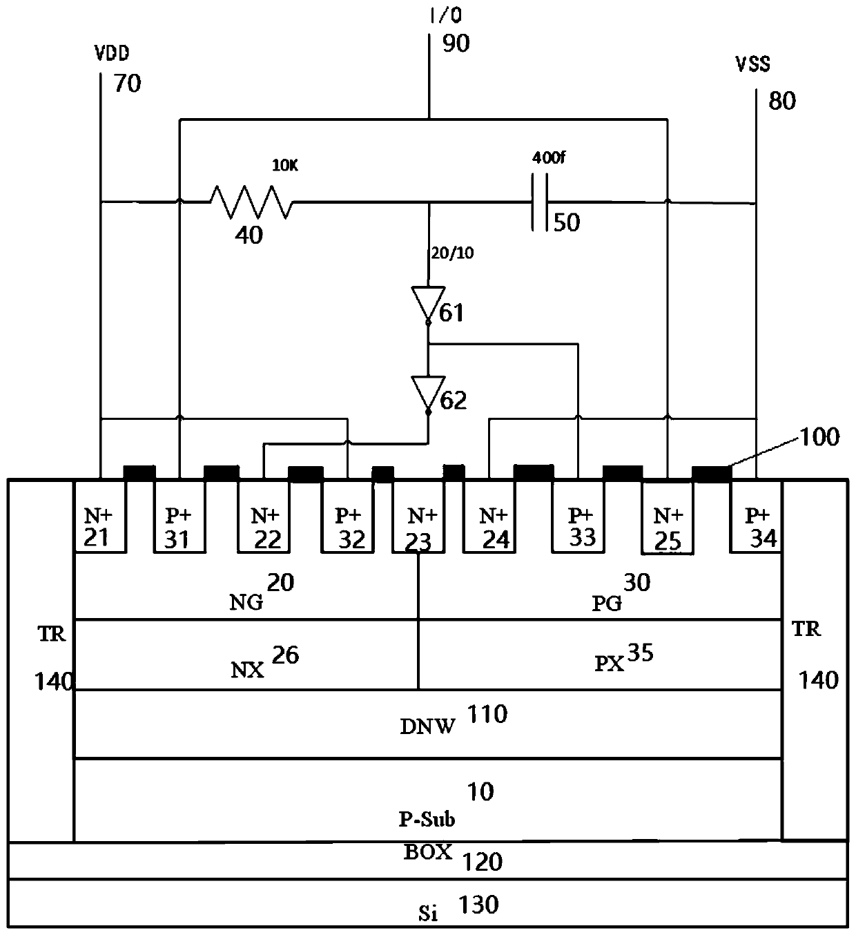
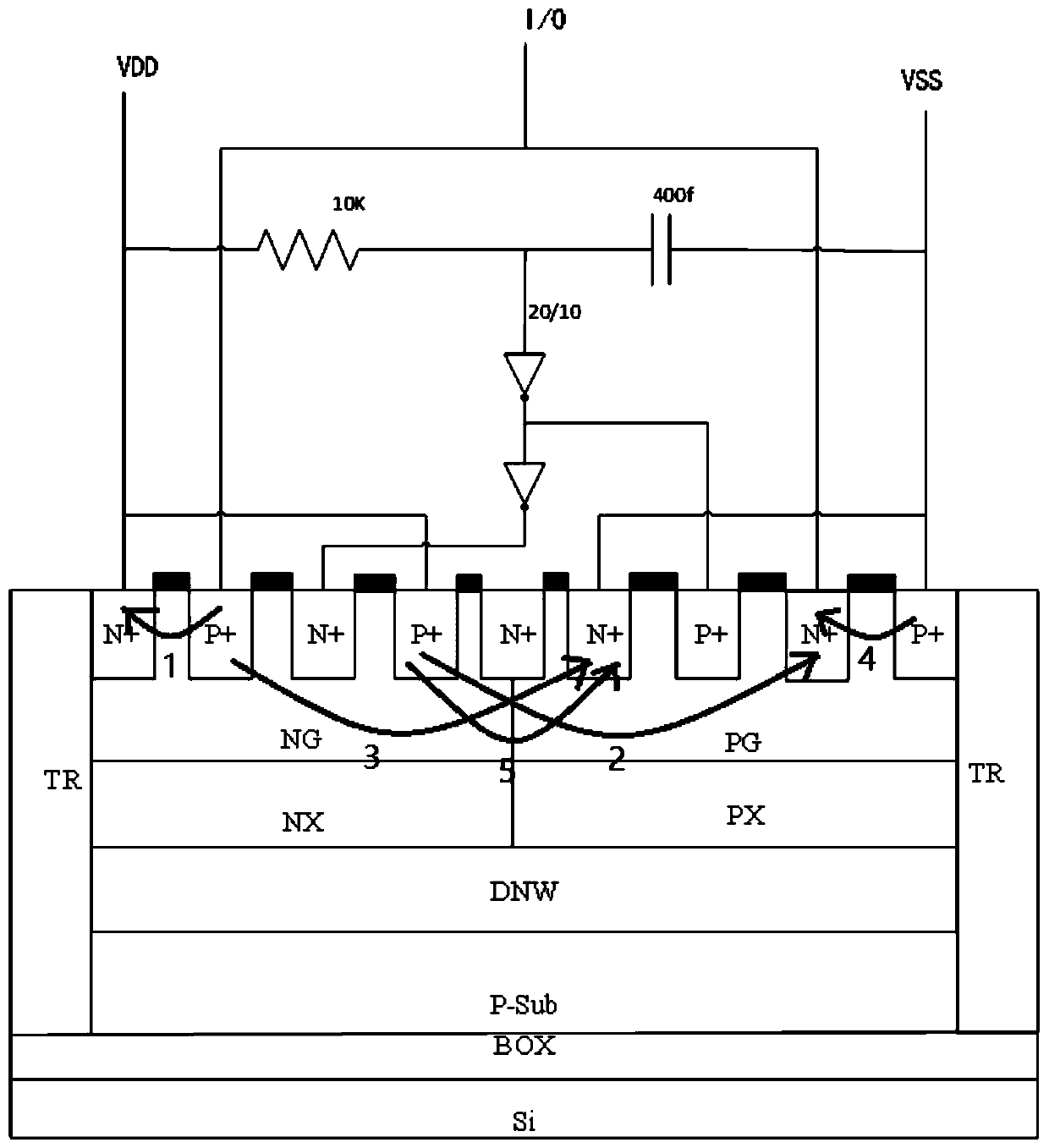
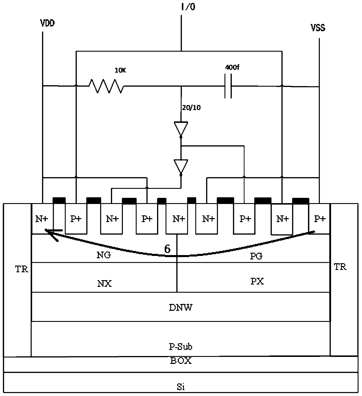
[0033] Hereinafter, embodiments of the present disclosure will be described with reference to the drawings. It should be understood, however, that these descriptions are exemplary only, and are not intended to limit the scope of the present disclosure. Also, in the following description, descriptions of well-known structures and techniques are omitted to avoid unnecessarily obscuring the concepts of the present disclosure.

[0034] Various structural schematic diagrams according to embodiments of the present disclosure are shown in the accompanying drawings. The figures are not drawn to scale, with certain details exaggerated and possibly omitted for clarity of presentation. The shapes of the various regions and layers shown in the figure, as well as their relative sizes and positional relationships are only exemplary, and may deviate due to manufacturing tolerances or technical limitations in practice, and those skilled in the art will Regions / layers with different shapes, ...


PUM


Abstract

The invention discloses an ESD protection structure, an integrated circuit and electronic equipment. The ESD protection structure comprises a first N well region and a first P well region which are sequentially connected and arranged on a top silicon layer; a first N+ region, a first P+ region, a second N+ region and a second P+ region located in the first N well region; a third N+ region positioned at the joint of the first N well region and the first P well region; a fourth N+ region, a third P+ region, a fifth N+ region and a fourth P+ region located in the first P well region; and a firstresistor, a first capacitor, a first inverter and a second inverter. According to the invention, the structure, the circuit and the equipment provided by the invention are used for solving the technical problems of incomplete protection circuits and too slow protection response existing in ESD protection of the integrated circuit in the prior art; and the ESD protection structure is comprehensivein protection and rapid in response.

Description

technical field [0001] The disclosure relates to the field of semiconductors, and in particular to an ESD protection structure, integrated circuits and electronic equipment. Background technique [0002] Electrostatic discharge (ESD, Electron Static Discharge) is an instantaneous process in which a large amount of static charge is poured into the integrated circuit from the outside to the inside when the pins of an integrated circuit are floating, and the whole process takes about 100ns. When the electrostatic discharge of the integrated circuit will generate hundreds or even thousands of volts of high voltage, the gate oxide layer of the input stage in the integrated circuit will be broken down. Damage to integrated circuits caused by electrostatic discharge is a well-known reliability problem. The continuous advancement of integrated circuit technology makes the feature size continue to decrease. On the one hand, it is beneficial to improve chip performance and reduce pr...

Claims


Application Information

Patent Timeline
Patent Type & Authority Applications(China)
IPC IPC(8): H01L27/02H02H9/04
CPCH01L27/0248H01L27/0296H01L27/0288H02H9/04H02H9/044H02H9/046
Inventor 夏瑞瑞蔡小五刘海南曾传滨赵海涛卜建辉高悦欣罗家俊
Owner INST OF MICROELECTRONICS CHINESE ACAD OF SCI
Why Eureka
Try Eureka