A Diamond Field-Effect Transistor with Air-Bridge-Like Source-Field Plate Structure

A field effect transistor and source field plate technology, applied in the field of diamond field effect transistors, can solve the problems of reducing the operating frequency, power gain, etc., and achieves improving the power gain and operating frequency, increasing the breakdown voltage, and reducing the gate-drain feedback capacitance. Effect

Active Publication Date: 2022-03-22
UNIV OF ELECTRONICS SCI & TECH OF CHINA
View PDF8 Cites 0 Cited by
  • Summary
  • Abstract
  • Description
  • Claims
  • Application Information

AI Technical Summary

Problems solved by technology

However, the traditional source field plate structure will increase the gate-source and gate-drain feedback capacitance, which will reduce the power gain and operating frequency

Method used


Image

  • A Diamond Field-Effect Transistor with Air-Bridge-Like Source-Field Plate Structure
  • A Diamond Field-Effect Transistor with Air-Bridge-Like Source-Field Plate Structure
  • A Diamond Field-Effect Transistor with Air-Bridge-Like Source-Field Plate Structure

Examples


Embodiment

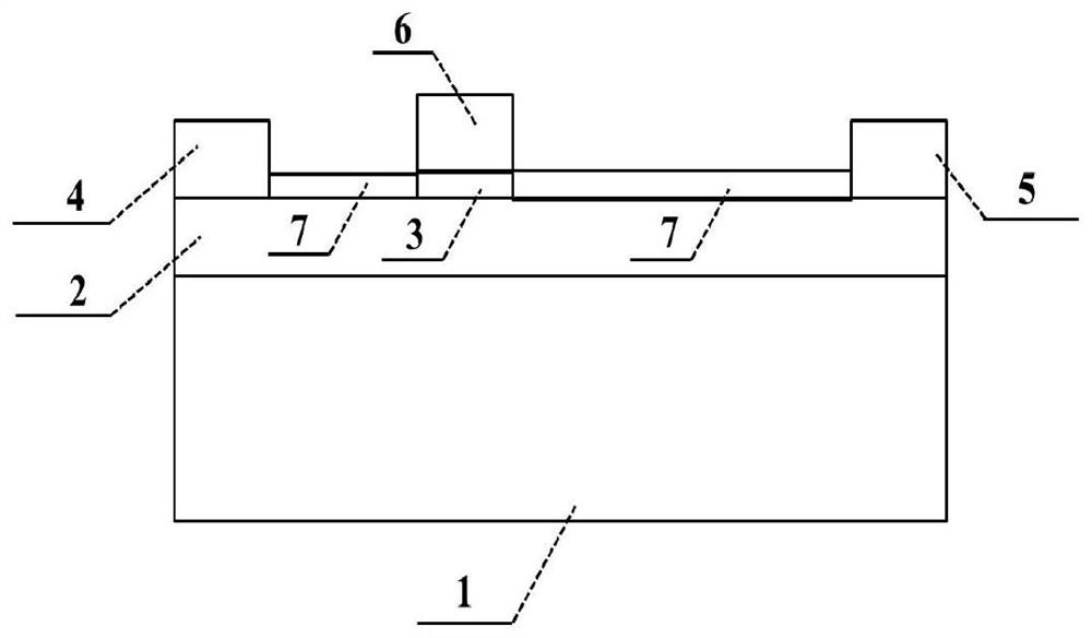
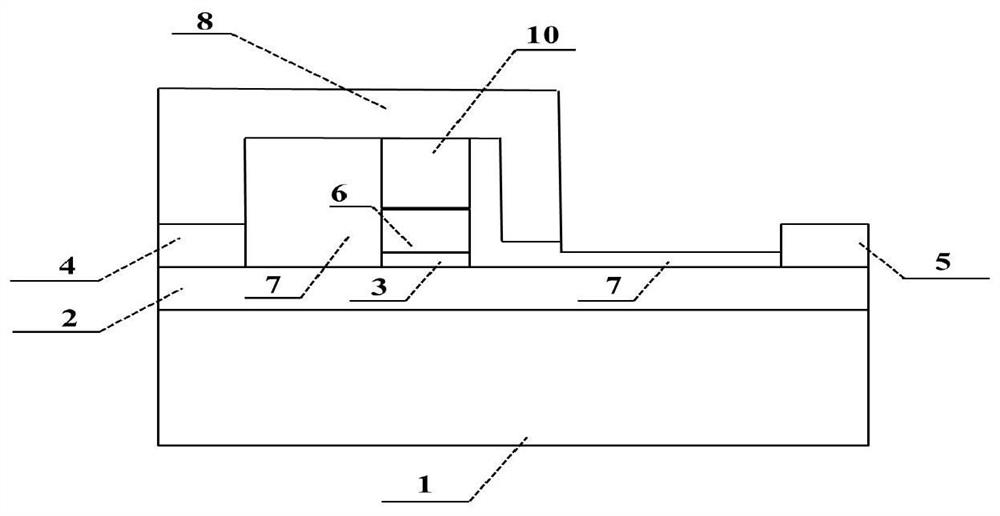
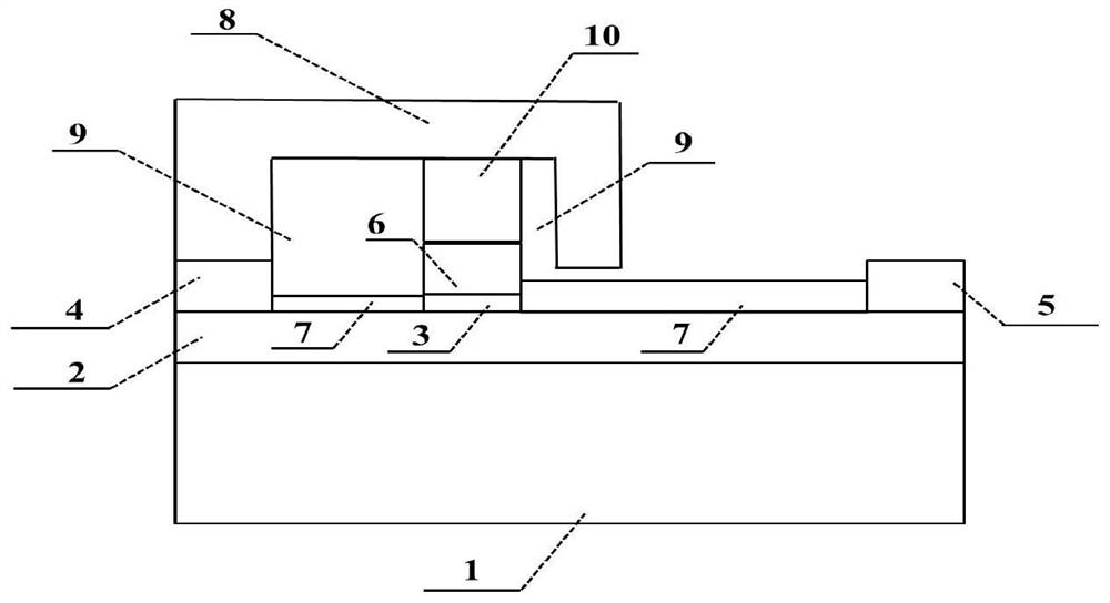
[0034] use image 3 Shown is a diamond field effect transistor with an air bridge type source field plate structure. The substrate layer 1 is crystal-oriented single-crystal diamond with a thickness of 1.9 μm; the epitaxial layer 2 is crystal-oriented single-crystal diamond with a thickness of 100 nm, a gate-source distance of 0.2 μm, a gate-drain distance of 1 μm, and a gate length of 0.2 μm. , the passivation layer 7, the gate dielectric layer 3 and the support layer 10 of the source field plate 8 on the gate electrode are all aluminum oxide, but the thickness of the passivation layer 7 in the gate source region and the passivation layer 7 in the gate drain region are different, respectively The thicknesses of the gate dielectric layer 3 and the support layer 10 of the source field plate on the gate electrode are 10nm and 320nm respectively. The distance between the bottom of the source field plate 8 of the gate and drain region and the passivation layer 7 is 10 nm, with an...


PUM

PropertyMeasurementUnit
thicknessaaaaaaaaaa
thicknessaaaaaaaaaa
thicknessaaaaaaaaaa

Abstract

The invention relates to a diamond field effect transistor with an air bridge type source field plate structure. The diamond field effect transistor includes: a substrate layer, an epitaxial layer, a gate dielectric layer, a source electrode, a drain electrode, a gate electrode, a passivation layer, a source field plate, an air layer and a support layer, the epitaxial layer is located on the substrate layer, and the epitaxial layer A source electrode and a drain electrode are arranged at both ends of the upper part, a gate electrode is arranged between the source electrode and the drain electrode, a gate dielectric layer is arranged between the gate electrode and the epitaxial layer, and a passivation layer is arranged on both sides of the gate dielectric layer, and the passivation layer is respectively connected to the epitaxial layer. The source electrode is in contact with the drain electrode, a supporting layer is arranged between the gate electrode and the source field plate, and an air layer is arranged between the passivation layer and the source field plate. The invention can reduce the grid-source feedback capacitance and the grid-drain feedback capacitance, improve the power gain and operating frequency, and simultaneously increase the breakdown voltage.

Description

technical field [0001] The invention relates to the field of diamond field effect transistors, in particular to a diamond field effect transistor with an air bridge-like source field plate structure. Background technique [0002] In terms of material properties, the third-generation semiconductor gallium nitride (GaN) has the advantages of large band gap, high critical breakdown electric field, high electron saturation velocity, and strong radiation resistance. Therefore, gallium nitride high electron mobility transistors (GaN HEMT) has strong ability of high frequency, pressure resistance, high temperature resistance and harsh environment. However, its thermal conductivity is still very low compared with diamond, and there are serious traps, so there is current collapse when outputting high power density, which seriously restricts the output capability of high power density. Due to its high breakdown voltage, high power density, high electron mobility, and high thermal con...

Claims


Application Information

Patent Timeline
Patent Type & Authority Patents(China)
IPC IPC(8): H01L29/06H01L29/40H01L29/78
CPCH01L29/0649H01L29/402H01L29/78
Inventor 徐跃杭陈志豪付裕吴韵秋
Owner UNIV OF ELECTRONICS SCI & TECH OF CHINA
Why Eureka
Try Eureka