Fabrication method of vertical double diffusion metal oxide semiconductor (VDMOS) device

A manufacturing method and device technology, applied in semiconductor/solid-state device manufacturing, semiconductor devices, electrical components, etc., can solve the problems of complex manufacturing process and inability to eliminate the influence of feedback capacitance well

Inactive Publication Date: 2017-09-15
PEKING UNIV FOUNDER GRP CO LTD +1
View PDF2 Cites 0 Cited by
  • Summary
  • Abstract
  • Description
  • Claims
  • Application Information

AI Technical Summary

Problems solved by technology

However, in the prior art, no matter whether the method of increasing the thickness of the gate oxide layer as a whole or the method of increasing the thickness of the gate oxide layer locally, it cannot well eliminate the influence of the feedback capacitance on VDMOS, and the manufacturing process is relatively complicated.

Method used


Image

  • Fabrication method of vertical double diffusion metal oxide semiconductor (VDMOS) device
  • Fabrication method of vertical double diffusion metal oxide semiconductor (VDMOS) device
  • Fabrication method of vertical double diffusion metal oxide semiconductor (VDMOS) device

Examples


Embodiment Construction

[0027] The following will clearly and completely describe the technical solutions in the embodiments of the present invention with reference to the accompanying drawings in the embodiments of the present invention. Obviously, the described embodiments are only some, not all, embodiments of the present invention. Based on the embodiments of the present invention, all other embodiments obtained by persons of ordinary skill in the art without making creative efforts belong to the protection scope of the present invention.

[0028] The terms "comprising" and "having" and any variations thereof in the description and claims of the present invention are intended to cover a non-exclusive inclusion, for example, a process comprising a series of steps or a device of structure need not be limited to the expressly listed Instead, those structures or steps may include other steps or structures not expressly listed or inherent to the process or device.

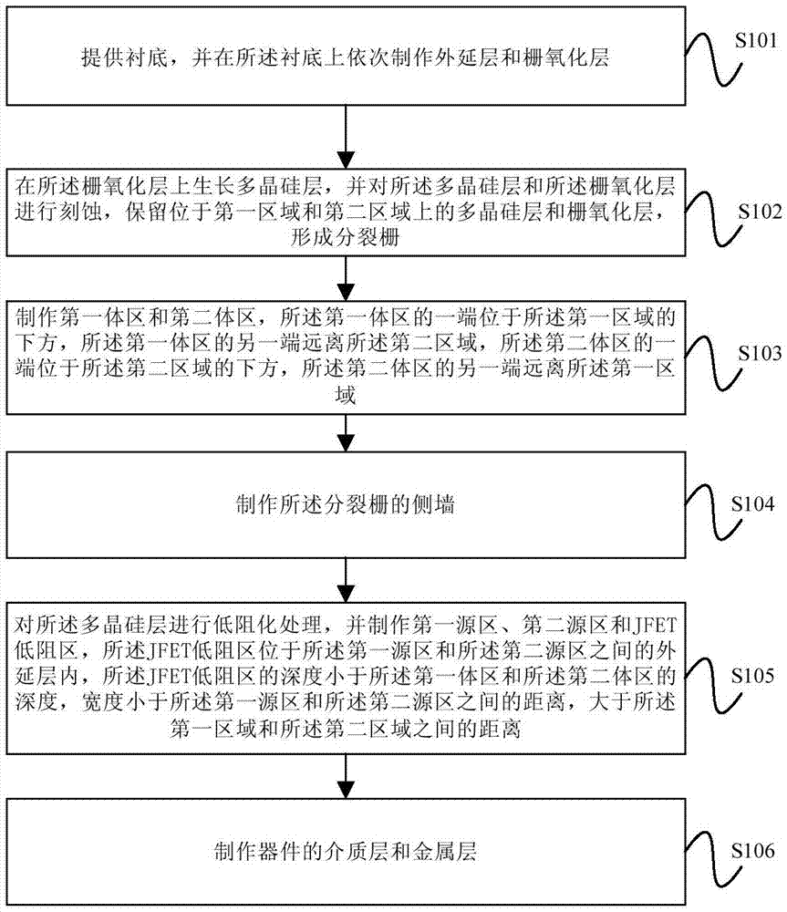
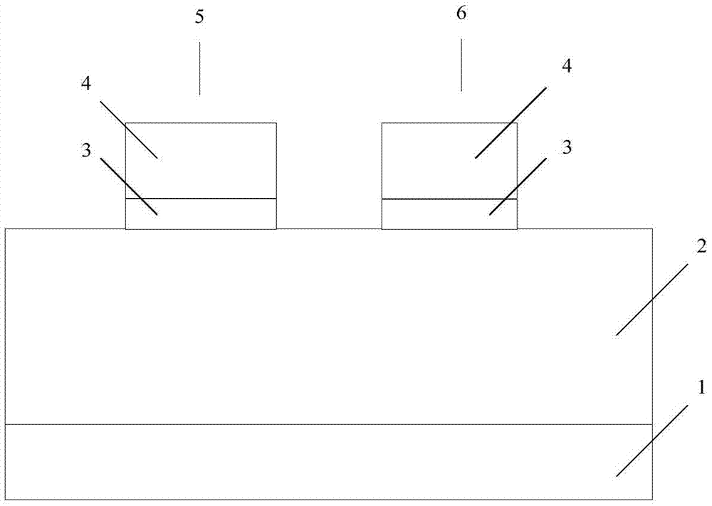
[0029] figure 1 A schematic flow c...


PUM


Abstract

The embodiment of the invention provides a fabrication method of a vertical double diffusion metal oxide semiconductor (VDMOS) device. The method comprises the steps of providing a substrate, and sequentially fabricating an epitaxial layer and a gate oxide layer on the substrate; growing a poly-silicon layer on the gate oxide layer, etching the poly-silicon layer and the gate oxide layer, and reserving the poly-silicon layer and the gate oxide layer on a first region and a second region to form split gates; fabricating a first body region and a second body region; fabricating side walls of the split gates; performing low-resistance processing on the poly-silicon layer, and fabricating a first active region, a second active region and a junction field-effect transistor (JFET) low-resistance region, wherein the JFET low-resistance region is arranged in the epitaxial layer between the first active region and the second active region, the depth of the JFET low-resistance region is smaller than the depths of the first body region and the second body region, and the width of the JFET low-resistance region is smaller than the distance between the first active region and the second active region and is larger than the distance between the first region and the second region; and fabricating a dielectric layer and a metal layer of the device. With the fabrication method of the VDMOS device, provided by the embodiment of the invention, the conduction resistance and the feedback capacitance of the VDMOS device can be reduced, and the performance of the device is improved.

Description

technical field [0001] Embodiments of the present invention relate to the technical field of semiconductor device manufacturing, and in particular, to a method for manufacturing a VDMOS device. Background technique [0002] Vertical double-diffused field-effect transistor (VDMOS) is one of the commonly used power transistors at present, and the feedback capacitance has always been the main factor affecting its performance. [0003] The method of reducing the feedback capacitance in the prior art mainly starts from reducing the oxide capacitance between the gate and the drain, such as increasing the thickness of the gate oxide layer as a whole or locally increasing the thickness of the gate oxide layer. However, in the prior art, no matter whether the method of increasing the thickness of the gate oxide layer as a whole or locally increases the thickness of the gate oxide layer, it cannot well eliminate the influence of the feedback capacitor on VDMOS, and the manufacturing p...

Claims


Application Information

Patent Timeline
IPC IPC(8): H01L21/336H01L29/423H01L29/10
CPCH01L29/66712H01L29/1095H01L29/42356
Inventor 赵圣哲
Owner PEKING UNIV FOUNDER GRP CO LTD
Why Eureka
Try Eureka