Semiconductor device

A semiconductor, conductive type technology, applied in the fields of semiconductor devices, semiconductor/solid-state device manufacturing, electrical components, etc., can solve the problems of reduced switching speed, large feedback capacitance, etc., to achieve the effect of reducing feedback capacitance

Inactive Publication Date: 2018-01-30
SANKEN ELECTRIC CO LTD
View PDF4 Cites 0 Cited by
  • Summary
  • Abstract
  • Description
  • Claims
  • Application Information

AI Technical Summary

Problems solved by technology

However, in trench gate type semiconductor devices, the capacitance between the gate electrode and the drain region (gate-drain capacitance), the capacitance between the gate electrode and the collector region (gate-collector capacitance) etc. The feedback capacitance is larger
Therefore, the switching speed decreases, causing problems in high-frequency operation

Method used


Image

  • Semiconductor device
  • Semiconductor device
  • Semiconductor device

Examples


other Embodiment approach

[0094] As mentioned above, although this invention was described using embodiment, it should not be understood that the description and drawing which make a part of this indication limit this invention. It is obvious that various alternative embodiments, examples, and applied techniques can be conceived by those skilled in the art from the present disclosure.

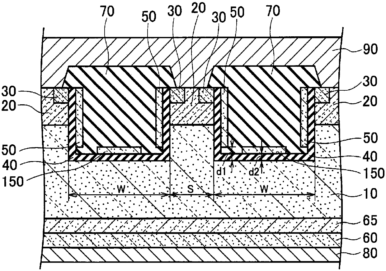
[0095] The above shows an example where the semiconductor device is an IGBT. However, the semiconductor device may also be a switching element of another trench gate type structure. Figure 14 An example in which the semiconductor device is a trench gate MOSFET is shown. Figure 14 The illustrated semiconductor device is a MOSFET having a structure in which an n-type drain region 160 is disposed on the lower surface of the drift region 10 . A drain electrode 180 electrically connected to the drain region 160 is disposed on the lower surface of the drain region 160 .

[0096] even if Figure 14 In the MOSFET semicond...


PUM


Abstract

The present invention provides a trench gate type semiconductor device that reduces the feedback capacitance generated at the bottom of the trough. The semiconductor device has a drift region (10); the base region (20), its configuration in the drift region (10); the emission region (30), its configuration in the base region (20); the inner wall of the insulating film (40), the configuration in the tank wall, the groove from the emitter region (30) on the surface and extends through the launch area (30) and the base (20); a gate electrode (50), and the base region (20) side of the insulating film on the inner wall of the side of the groove in the allocation of land (40); the bottom surface of the electrode (150), and the gate electrode (50) insulation the separation configuration of bottomgroove of the inner wall of the insulating film (40); and an interlayer insulating film (70), (50) arranged on the gate electrode and the bottom electrode (150) between the gate electrode (50), fromthe surface to at least a portion of the slot The distance between the bottom and the bottom is longer than at least a part of the lower surface of the bottom surface electrode (150) to the bottom ofthe groove.

Description

technical field [0001] The present invention relates to trench gate semiconductor devices. Background technique [0002] A power MOSFET, an insulated gate bipolar transistor (IGBT), or the like is used as a switching element (power semiconductor element) that performs a switching operation of a large current. These switching elements employ a trench-type gate electrode structure (trench gate type), in which a gate insulating film and a gate electrode are formed in a groove (trench) formed in a semiconductor substrate. However, in trench gate semiconductor devices, the capacitance between the gate electrode and the drain region (gate-drain capacitance), the capacitance between the gate electrode and the collector region (gate-collector capacitance) etc. The feedback capacitance is larger. Therefore, the switching speed decreases, causing a problem in high-frequency operation. [0003] Various methods for reducing the feedback capacitance are being investigated. For exampl...

Claims


Application Information

Patent Timeline
IPC IPC(8): H01L29/78H01L29/739H01L29/423H01L21/336H01L21/331
Inventor 川尻智司
Owner SANKEN ELECTRIC CO LTD
Why Eureka
Try Eureka